Diese
Erfindung betrifft einen optischen Schalter, der bei ultraschnellen
Schaltraten betrieben werden kann.These
The invention relates to an optical switch used in ultrafast
Switching rates can be operated.
Jüngste Entwicklungen
bei Femtosekundenlasern und optischen Signalverarbeitungstechniken haben
die Erzeugung ultraschneller optischer Pulse erlaubt, und Pulsbreiten
von weniger als 100 fs können
nun routinemäßig erzeugt
werden. Bei einem optischen Schalter treten jedoch Schwierigkeiten
bei der Bereitstellung eines Schaltmediums auf, welches genau so
schnell wie die verfügbaren
Pulse betrieben werden kann und gleichzeitig nur eine geringe Schaltenergie
benötigt.Recent developments
in femtosecond lasers and optical signal processing techniques
allows the generation of ultrafast optical pulses, and pulse widths
of less than 100 fs
now routinely generated
become. However, difficulties arise in an optical switch
in the provision of a switching medium on which exactly
fast as the available
Pulse can be operated while only a small switching energy
needed.
In
der EP-A-0744648 [Art. 54(3) EPC] ist ein optischer Schalter beschrieben,
bei dem erste und zweite kohärente
Pulse eingesetzt werden, um ein optisches Medium zwischen verschiedenen
angeregten Zuständen
zu schalten, um seine optischen Transmissionseigenschaften zu verändern. Dieses Konzept
ist ebenfalls beschrieben in Physical Review Letters, 25. September
1995, USA, Band 15 Nr. 13, Seiten 2598–2607, Herbele A. P. et al. "Ultrafast coherent
control and destruction of excitons in quantum wells".In
EP-A-0744648 [Art. 54 (3) EPC] an optical switch is described,
at the first and second coherent
Pulse can be used to make an optical medium between different
excited states
to change its optical transmission properties. This concept
is also described in Physical Review Letters, 25th September
1995, USA, Vol. 15, No. 13, pp. 2598-2607, Herbele A.P. et al. "Ultrafast coherent
control and destruction of excitons in quantum wells ".
Ein
Alternativansatz, der die Spincharakteristika von fotoangeregten
Ladungsträgern
verwendet, ist beschrieben in "All-optical
picosecond switching of a quantum well etalon using spin-polarisation relaxation", Y. Nishikawa et
al., Appl. Phys. Lett., 66, 839 (1995). Bei dieser Technik wird
ein zirkular polarisierter optischer Puls auf das Schaltmedium gerichtet,
welches ein Elektron-Loch-Paar durch Fotoanregung erzeugt, wobei
das Elektron und das Loch unterschiedliche Spinzustände haben.
Das Loch zerfällt relativ
schnell, wohingegen der Elektronenspinzustand etwas länger bestehen
bleibt, mehr als einige Pikosekunden. Das Schaltmedium umfasst eine
periodische Struktur aus Quantentöpfen. Der resultierende Spinzustand
wird mittels eines Pulses von linear polarisierter optischer Prüfstrahlung
erfasst, und es wurde festgestellt, dass die Polarisationsebene
während
des Auftretens des angehobenen Elektronenspinzustands gedreht wird.
Die Polarisationsebene des Prüfpulses
wird somit erfasst, um eine Ausgabe für den optischen Schalter zu
liefern. Zum Zurücksetzen
verlässt
sich der Spinzustandsschalter somit auf die natürliche Spinrelaxation der Elektronen
in der Quantentopfstruktur, was die erreichbare Schaltbetriebsgeschwindigkeit
begrenzt. Zur Beschleunigung der Rate wurde vorgeschlagen, optisch
inaktive Quantentöpfe
angrenzend an jene bereitzustellen, in denen die erhöhten Ladungsträgerspinzustände induziert
werden, um ein Tunneln der Ladungsträger in die inaktiven Töpfe zu ermöglichen.
In der Praxis führt
dies jedoch nicht zu einer guten Kontrolle über die Schalteigenschaften.One
Alternative approach, which has the spin characteristics of photoexcited
carriers
used is described in "All-optical
picosecond switching of a quantum well etalon using spin-polarization relaxation ", Y. Nishikawa et
al., Appl. Phys. Lett., 66, 839 (1995). This technique will
a circularly polarized optical pulse directed to the switching medium,
which produces an electron-hole pair by photo-excitation, wherein
the electron and the hole have different spin states.
The hole disintegrates relatively
fast, whereas the electron spin condition is slightly longer
stays, more than a few picoseconds. The switching medium comprises a
periodic structure of quantum wells. The resulting spin state
is determined by means of a pulse of linearly polarized optical test radiation
recorded, and it was found that the polarization plane
while
the occurrence of the raised electron spin state is rotated.
The polarization plane of the test pulse
is thus detected to be an output for the optical switch
deliver. To reset
leaves
The spin state switch thus focuses on the natural spin relaxation of the electrons
in the quantum well structure, what the achievable switching operating speed
limited. To speed up the rate was suggested optically
inactive quantum wells
adjacent to those in which the enhanced charge carrier spin states induce
to allow tunneling of the charge carriers into the inactive pots.
In practice leads
but not to good control over the switching properties.
Die US 5151589 von Takeuchi
beschreibt einen optischen Schalter zum Modulieren eines zirkular
polarisierten Lichtstrahls mit einem anderen. Allerdings ist die
Schaltgeschwindigkeit auf die Spinrelaxationszeit begrenzt, denn
sobald die Probe angeregt worden ist, muss der überschüssige Spin relaxieren, bevor
die Probe erneut angeregt werden kann.The US 5151589 by Takeuchi describes an optical switch for modulating a circularly polarized light beam with another. However, the switching speed is limited to the spin relaxation time, because once the sample has been excited, the excess spin must relax before the sample can be re-excited.
Gemäß der vorliegenden
Erfindung wird ein optischer Spinschalter positiv zwischen zwei
verschiedenen Spinzuständen
umgeschaltet.According to the present
Invention, an optical spin switch is positive between two
different spin states
switched.
Erfindungsgemäß wird ein
optischer Schalter bereitgestellt, umfassend ein optisches Schaltmedium,
eine Pulsquelle, um einen ersten Puls von optischer Strahlung mit
einer ersten Polarisationscharakteristik auf das Schaltmedium zu
richten, um eine erste Ladungsträger-Spinzustandsbedingung
zu erzeugen, eine Pulsquelle, um danach einen zweiten Puls von optischer
Strahlung mit einer unterschiedlichen Polarisationscharakteristik
vor einer Relaxation der ersten Ladungsträger-Spinzustandsbedingung auf das
Schaltmedium zu richten, um eine zweite Ladungsträger-Spinzustandsbedingung
zu erzeugen, und eine Prüfstrahlungsquelle,
um optische Prüfstrahlung
in das Medium zu richten, um die Spinzustandsbedingung des Mediums
zu bestimmen.According to the invention is a
optical switch provided, comprising an optical switching medium,
a pulse source to receive a first pulse of optical radiation
a first polarization characteristic to the switching medium
to determine a first carrier spin state condition
to generate a pulse source, followed by a second pulse of optical
Radiation with a different polarization characteristic
prior to relaxation of the first carrier spin state condition on the
Switching medium to a second carrier spin state condition
and a test radiation source,
for optical test radiation
in the medium to the spin state condition of the medium
to determine.
Der
erste Puls kann eine Polarisation haben, die zeitlich in einer ersten
Richtung rotiert, und ein zweiter Puls kann eine Polarisation haben,
die in einer zweiten entgegengesetzten Richtung rotiert. Der erste
und der zweite Puls können
zirkular polarisiert sein.Of the
first pulse can have a polarization, which in time in a first
Direction is rotating, and a second pulse may have a polarization,
which rotates in a second opposite direction. The first
and the second pulse can
be circularly polarized.
Der
Schalter kann eine Detektoreinrichtung umfassen, die auf Polarisationscharakteristika
der Prüfstrahlung
nach ihrem Durchgang in das Schaltmedium anspricht, um den Spinzustand
des Mediums zu erfassen. Die Prüfstrahlung
kann gepulst sein, und kann linear polarisiert sein, so dass Änderungen
ihrer Polarisationsrichtung eine Funktion des Spinzustands des Schaltmediums
sind.Of the
Switch may include a detector device based on polarization characteristics
the test radiation
after its passage into the switching medium responds to the spin state
of the medium. The test radiation
can be pulsed, and can be linearly polarized, making changes
its polarization direction is a function of the spin state of the switching medium
are.
Züge des ersten
und des zweiten Pulses und der Prüfstrahlung können auf
das Medium gerichtet werden, und der Schalter kann dann derart betrieben werden,
dass die Detektoreinrichtung eine Ausgabe als Funktion der Wiederholfrequenzen
und relativen Phasen der Pulszüge
liefert. Der Schalter kann somit in einer phasenempfindlichen Detektoranordnung verwendet
werden, bei der die Ausgabe der Detektoreinrichtung verwendet wird,
um die Phase der Prüfpulse
relativ zur Phase der ersten und zweiten Pulse zu kontrollieren.Trains of the first
and the second pulse and the test radiation can on
the medium can be directed, and the switch can then be operated in such a way
that the detector means an output as a function of the repetition frequencies
and relative phases of the pulse trains
supplies. The switch can thus be used in a phase-sensitive detector arrangement
where the output of the detector device is used,
around the phase of the test pulses
relative to the phase of the first and second pulses.
Ein
Magnetfeld kann an das Schaltmedium angelegt werden, um dafür zu sorgen,
dass die durch den ersten Puls induzierten Ladungsträgerspins
in Richtung einer Ausrichtung mit den durch den zweiten Puls induzierten
Ladungsträgerspins
präzessieren.
Dies kann verwendet werden, um den Grad der Korrelation zwischen
den Pulszügen
zu bestimmen. Die Stärke
des Magnetfelds kann zeitlich variiert werden, um eine Spitze in
der Detektorausgabe zu erzeugen, und die Feldstärke der Spitze liefert somit ein
Maß für die Pulszugkorrelation.A magnetic field can be transmitted to the switching medium to precess that the charge carrier spins induced by the first pulse precess in the direction of alignment with the charge carrier spins induced by the second pulse. This can be used to determine the degree of correlation between the pulse trains. The strength of the magnetic field may be varied over time to produce a peak in the detector output, and the field strength of the peak thus provides a measure of the pulse train correlation.
Die
Detektoreinrichtung kann so betrieben werden, dass sie eine Ausgabe
als Funktion einer Zeitverzögerung
zwischen den ersten und zweiten Pulsen liefert, die alternativ als
zeitliches Integral des Spinzustands angesehen werden kann, der
im Schaltmedium auftritt. Die in diesem Beispiel verwendete Prüfstrahlung
kann eine Pulsdauer haben, die beträchtlich länger als die Pulsdauer für die ersten und
zweiten Pulse ist. Die Prüfstrahlung
kann kontinuierliche Strahlung enthalten, beispielsweise aus einer
Laserquelle.The
Detector device may be operated to output
as a function of a time delay
between the first and second pulses, alternatively as
temporal integral of the spin state can be considered, the
occurs in the switching medium. The test radiation used in this example
can have a pulse duration that is considerably longer than the pulse duration for the first and second
second pulse is. The test radiation
may contain continuous radiation, for example from one
Laser source.
Eine
solche Anordnung kann zur Datenübertragung
eingesetzt werden, wobei eine Datencodiereinrichtung Daten durch
Kontrollieren der Verzögerung
zwischen den ersten und zweiten Pulsen codiert.A
such arrangement may be for data transmission
be used, wherein a data encoding device by data
Control the delay
encoded between the first and second pulses.
Zur
Erhöhung
des Kontrasts zwischen den Spinzustandsbedingungen des Schalters
kann das Schaltmedium in einem optischen Resonanzhohlraum enthalten
sein. Das Schaltmedium kann eine Quantentopfstruktur enthalten,
die einen ersten Topf für
Ladungsträger
in der ersten Spinzustandsbedingung sowie einen zweiten Topf enthält, der
vom ersten Topf durch eine Barriereeinrichtung getrennt ist, durch
welche Ladungsträger
aus dem ersten Topf tunneln können,
um einen langlebigen Ladungsträgeraufbau
im ersten Topf zu vermeiden. Die Quantentopfstruktur kann eine periodische
Struktur von Schichten aus GaAs- und AlGaAs-Material enthalten, obwohl
weitere Materialsysteme verwendet werden können, wie aus den nachfolgend
beschriebenen detaillierten Beispielen deutlich wird:to
increase
the contrast between the spin state conditions of the switch
may contain the switching medium in an optical resonant cavity
be. The switching medium may contain a quantum well structure,
the first pot for
charge carrier
in the first spin state condition and a second pot containing
from the first pot is separated by a barrier device through
which charge carriers
can tunnel out of the first pot,
for a long-lasting charge carrier structure
to avoid in the first pot. The quantum well structure may be periodic
Structure of layers of GaAs and AlGaAs material included, though
other material systems can be used, as shown in the following
becomes clear in the following detailed examples:
Damit
die Erfindung vollständiger
verstanden wird, wird eine Ausführungsform
derselben nun als erläuterndes
Beispiel mit Bezug zu den beigefügten Zeichnungen
beschrieben werden, in denen:In order to
the invention more complete
is understood, becomes an embodiment
the same now as an explanatory
Example with reference to the accompanying drawings
be described, in which:
1 eine
schematische Darstellung eines erfindungsgemäßen optischen Schalters ist; 1 a schematic representation of an optical switch according to the invention is;
2 eine
schematische Querschnittsansicht des in 1 gezeigten
optischen Schaltmediums ist; 2 a schematic cross-sectional view of the in 1 shown optical switching medium;
3 ein
Energie-Spin-Diagramm für
die im optischen Schaltmedium induzierten optischen Übergänge ist; 3 is an energy-spin diagram for the optical transitions induced in the optical switching medium;
4 ein
schematisches Vektordiagramm ist, welches zeigt, dass der linear
polarisierte Prüfpuls
als zwei Pulse aufgefasst werden kann, die in entgegengesetzten
Richtungen zirkular polarisiert sind; 4 Fig. 12 is a schematic vector diagram showing that the linearly polarized probe pulse can be considered as two pulses that are circularly polarized in opposite directions;
5 den
Effekt der erste Spinzustandsbedingung des optischen Schaltmediums
auf die Polarisation des Prüfpulses
erläutert; 5 explains the effect of the first spin state condition of the optical switching medium on the polarization of the test pulse;
6 ein
Graph des gesamten Trägerspins als
Funktion der Zeit in Antwort auf verschiedene Verzögerungen
zwischen den ersten und zweiten Kontrollpulsen ist; 6 is a graph of the total carrier spin as a function of time in response to various delays between the first and second control pulses;
7 eine
Alternativform des Detektors erläutert; 7 an alternative form of the detector explained;
8 eine
Konfiguration erläutert,
in der die Prüfpulse
durch das optische Schaltmedium hindurch transmittiert werden; 8th explains a configuration in which the test pulses are transmitted through the optical switching medium;
9 eine
schematische Darstellung der in 1 gezeigten
Kontrollpulsquelle ist; 9 a schematic representation of in 1 shown control pulse source;
10 eine
schematische Querschnittsansicht eines optischen Schaltmediums mit
einer asymmetrischen Topfkonfiguration ist; 10 Fig. 12 is a schematic cross-sectional view of an optical switching medium having an asymmetric pot configuration;
11 ein
Energiediagramm für
die in 10 gezeigten Töpfe ist; 11 an energy diagram for the in 10 shown pots is;
12 die
innerhalb eines optischen Mikrohohlraums angeordneten Quantentöpfe erläutert; 12 explains the quantum wells disposed within an optical microvoid;
13 eine
schematische Darstellung einer Modifikation des Schalters ist, bei
der ein Magnetfeld parallel zu den Quantentöpfen angelegt wird, um eine Präzession
der Elektronenspins zur Verwendung bei einer Kreuzkorrelation von
Pulsströmen
zu erzeugen; 13 Fig. 12 is a schematic representation of a modification of the switch in which a magnetic field is applied in parallel with the quantum wells to produce precession of the electron spins for use in cross-correlation of pulse currents;
14 ein
schematisches Vektordiagramm der Elektronenspinpräzession
ist; 14 is a schematic vector diagram of the electron spin precession;
15a ein Graph des Spinzustands des optischen Schaltmediums
als Funktion der Zeit in Antwort auf erste und zweite rechts und
links zirkular polarisierte Pulse in Anwesenheit eines schwachen Felds
ist; 15a Figure 12 is a graph of the spin state of the optical switching medium as a function of time in response to first and second right and left circularly polarized pulses in the presence of a weak field;
15b ein Graph entsprechend 15a ist,
jedoch bei Anwesenheit eines starken Felds; 15b a graph accordingly 15a but in the presence of a strong field;
16 verschiedene Wellenformen darstellt,
um den Betrieb eines phasenempfindlichen Detektors zu erklären, der
einen erfindungsgemäßen Schalter
benutzt; 16 illustrate various waveforms to explain the operation of a phase sensitive detector using a switch according to the invention;
17 ein
schematisches Diagramm eines optischen Datenübertragungssystems ist, das
einen erfindungsgemäßen Schalter
benutzt; und 17 Fig. 10 is a schematic diagram of an optical communication system using a switch according to the invention; and
18 die
optische Pulskonfiguration erläutert,
die zum Codieren der im Gerät
von 17 übertragenen
Daten benutzt wird. 18 explained the optical pulse configuration used to encode the device in the 17 transmitted data is used.
Mit
Bezug auf 1 besteht die Schaltvorrichtung
aus einem optischen Schaltmedium 1 in Form einer Halbleiter-Quantentopfstruktur,
auf die Steuerpulse aus einer Steuerpulsquelle 2 auf einen Weg 3 gerichtet
werden. Die Steuerpulse schalten den Spinzustand von Ladungsträgern im
optischen Schaltmedium 1 um, und der resultierende Spinzustand
des Mediums wird mit Hilfe eines Prüfpulses P aus einer Prüfstrahlungsquelle 4 erfasst,
der entlang eines Wegs 5 in das Medium 1 gerichtet
wird. Die Prüfpulse
aus der Quelle 4 sind linear polarisiert und verlaufen
durch einen Polarisationsstrahlteiler 6, wenn sie zum optischen
Schaltmedium 1 laufen. Wie nachfolgend detaillierter beschrieben
wird, wird die Polarisationsebene des Prüfpulses abhängig vom Spinzustand des optischen
Schaltmediums gedreht, so dass vom Medium 1 reflektierte
Prüfpulse
durch den Strahlteiler mit einer Amplitude reflektiert werden, die
vom Betrag der Drehung der Polarisationsebene abhängt, und
zwar entlang eines Wegs 7 zu einem Detektor 8,
der ein elektrisches Signal mit einer Amplitude erzeugt, die vom
Grad der Drehung der Polarisationsebene des Prüfpulses durch das Halbleitermedium
abhängt.
Die Ausgabe des Detektors 8 wird einem elektrischen Verstärker 9 zugeführt, um ein
Ausgangssignal auf einer Leitung 10 bereitzustellen.Regarding 1 If the switching device consists of an optical switching medium 1 in the form of a semiconductor quantum well structure, to the control pulses from a control pulse source 2 on a way 3 be directed. The control pulses switch the spin state of charge carriers in the optical switching medium 1 and the resulting spin state of the medium is detected by means of a test pulse P from a test radiation source 4 captured along a path 5 into the medium 1 is directed. The test pulses from the source 4 are linearly polarized and pass through a polarization beam splitter 6 if it is the optical switching medium 1 to run. As described in more detail below, the polarization plane of the test pulse is rotated depending on the spin state of the optical switching medium, so that the medium 1 reflected test pulses are reflected by the beam splitter with an amplitude that depends on the amount of rotation of the polarization plane, along a path 7 to a detector 8th which generates an electrical signal having an amplitude which depends on the degree of rotation of the polarization plane of the test pulse through the semiconductor medium. The output of the detector 8th becomes an electric amplifier 9 fed to an output signal on a line 10 provide.
Die
Steuerpulsquelle 2 erzeugt erste und zweite optische Pulse
CP1, CP2, die zeitlich durch eine Verzögerung T getrennt sind. Die
Steuerpulse CP1, CP2 sind in entgegengesetzten Richtungen zirkular
polarisiert. In diesem Beispiel ist der Puls CP1 rechtshändig zirkular
polarisiert (rcp), wohingegen der zweite Steuerpuls CP2 linkshändig zirkular
polarisiert ist (lcp). Der erste Steuerpuls CP1 schaltet das optische
Schaltmedium in einen ersten Spinzustand, und der zweite Puls CP2
schaltet das Medium 1 anschließend in einen zweiten, unterschiedlichen
Spinzustand, wie nachfolgend detaillierter beschrieben wird.The control pulse source 2 generates first and second optical pulses CP1, CP2 separated in time by a delay T. The control pulses CP1, CP2 are circularly polarized in opposite directions. In this example, the pulse CP1 is right-handed circularly polarized (rcp), whereas the second control pulse CP2 is left-handed circularly polarized (lcp). The first control pulse CP1 switches the optical switching medium into a first spin state, and the second pulse CP2 switches the medium 1 subsequently into a second, different spin state, as described in more detail below.
Das
optische Schaltmedium 1 umfasst in diesem Beispiel eine
in 2 detaillierter gezeigte Mehrfachschicht-Quantentopfstruktur,
die ein Substrat aus GaAs-Material 11 umfasst, auf dem
Schichten aus AlGaAs und GaAs durch Molekularstrahlepitaxie (MBE)
oder andere geeignete Techniken gebildet sind, um eine periodische
Topfstruktur zu bilden. In diesem Beispiel wurden fünf GaAs-Quantentöpfe aus Schichten 12, 13 aus
GaAs und AlGaAs-Material hergestellt. In diesem Beispiel haben die
GaAs-Quantentöpfe
eine Dicke von 25 nm.The optical switching medium 1 includes in this example a in 2 In more detail, a multi-layer quantum well structure, which is a substrate of GaAs material 11 on which layers of AlGaAs and GaAs are formed by molecular beam epitaxy (MBE) or other suitable techniques to form a periodic pot structure. In this example, five GaAs quantum wells were made up of layers 12 . 13 made of GaAs and AlGaAs material. In this example, the GaAs quantum wells have a thickness of 25 nm.
Der
Effekt der Steuerpulse CP1, CP2 auf das optische Medium kann anhand
des Spin-Energie-Diagramms der 3 gesehen
werden. Der rechtshändig
zirkular polarisierte Puls CP1 erzeugt ein Exciton, bei dem ein
Elektron auf ein Energieniveau E1 im Leitungsband angehoben wird
und ein Loch im Valenzband zurücklässt, wie
durch den Pfeil 14 gezeigt ist. Das Elektron im Energiezustand
E1 hat einen Spin von –1/2
und das entsprechende Loch hat einen Spin von –3/2. Der Lochspin wird verhältnismäßig rasch
in den +3/2-Zustand gestreut, doch das Elektron im Spinzustand –1/2 hat
eine Spinlebensdauer in der Größenordnung
von mehreren Pikosekunden. In Antwort auf den ersten Steuerpuls
CP1 wird somit das optische Medium 1 in einen ersten Spinzustand
mit Elektronen bei der Energie E1 mit einem Spin –1/2 angehoben.
Erfindungsgemäß wurde
festgestellt, dass das Medium mit Hilfe des zweiten Steuerpulses CP2
mit einer zum ersten Puls entgegengesetzten zirkularen Polarisation
in einen zweiten Spinzustand geschaltet werden kann. In 3 erzeugt
der Puls CP2 einen Übergang 15,
bei dem ein Elektron auf die Energie E1 mit einem Spin +1/2 angehoben
wird, wobei ein Loch mit Spin +3/2 im Valenzband gebildet wird.
Die Zeitverzögerung
T zwischen dem ersten und dem zweiten Puls CP1, CP2 ist kleiner
als die Relaxationszeit τ der
Elektronen bei der Energie E1, so dass der Gesamteffekt der Elektronen
mit Spin –1/2
und +1/2, der durch die Pulse CP1 und CP2 erzeugt wird, ein Gesamtspinzustand
von 0 ist. Somit wird das optische Schaltmedium anfänglich durch den
Puls CP1 in einen ersten Spinzustand von +1/2, geschaltet und danach
in einer Zeit, die kleiner als die Relaxationszeit τ des Energiezustands
ist, wird es durch den Puls CP2 in einen zweiten Zustand mit Null-Nettospin geschaltet.The effect of the control pulses CP1, CP2 on the optical medium can be determined by the spin-energy diagram of FIG 3 be seen. The right-hand circularly polarized pulse CP1 produces an exciton in which an electron is raised to an energy level E1 in the conduction band and leaves a hole in the valence band, as indicated by the arrow 14 is shown. The electron in energy state E1 has a spin of -1/2 and the corresponding hole has a spin of -3/2. The hole spin is scattered relatively rapidly in the + 3/2 state, but the spin-state electron -1/2 has a spin lifetime of the order of several picoseconds. In response to the first control pulse CP1 thus becomes the optical medium 1 raised to a first spin state with electrons at energy E1 with a -1/2 spin. According to the invention, it has been found that the medium can be switched into a second spin state with the aid of the second control pulse CP2 with a circular polarization opposite to the first pulse. In 3 the pulse CP2 generates a transition 15 in which an electron is raised to the energy E1 with a spin +1/2, forming a hole with spin +3/2 in the valence band. The time delay T between the first and second pulses CP1, CP2 is less than the relaxation time τ of the electrons at the energy E1, so that the total effect of the electrons with spin -1/2 and +1/2 caused by the pulses CP1 and CP2 is generated, is a total spin state of 0. Thus, the optical switching medium is initially switched to a first spin state of +1/2 by the pulse CP1, and thereafter in a time smaller than the relaxation time τ of the energy state, it is changed to a second state with zero by the pulse CP2. Nettospin switched.
Der
Spinzustand des optischen Schaltmediums steuert die Polarisation
des Prüfpulses
aus der Quelle 4 (1). Mit
Bezug zu 4 ist der Prüfpuls P linear polarisiert,
wie bei 16 gezeigt, und man kann erkennen, dass die lineare
Polarisation aus zwei zirkularen Polarisationen entgegengesetzter
Händigkeit aufgebaut
ist, wie durch die Vektoren C1 und C2 erläutert wird. Diese zirkularen
Polarisationen koppeln mit den in 3 gezeigten
Spinzuständen.
Der Übergang 14 zwischen
Löchern
mit Spin +3/2 und Elektronen mit Spin +1/2 induziert eine optische
Nichtlinearität
hauptsächlich
für linkszirkular
polarisiertes Licht. Ähnlich
verursacht der Übergang 15 von 3 eine Nichtlinearität hauptsächlich für rechtszirkular
polarisiertes Licht. Wenn somit das optische Schaltmedium in der
ersten Spinzustandsbedingung in Antwort auf den Puls CP1 ist, wird
die Zirkularkomponente C2 des Prüfpulses
P im Medium derart absorbiert, dass die in 5 gezeigte
Bedingung erzeugt wird, bei der die Amplitude der zirkularen Polarisationskomponente
C2 auf C2' verringert
ist. Die Vektorsumme P' der zwei
Zirkularpolarisationen C1 und C2' ist
in 5b gezeigt. Wenn somit der Prüfpuls zwischen dem Auftreten
des ersten und des zweiten Pulses CP1 und CP2 in das Schaltmedium
gerichtet wird, wird sein Polarisationsvektor ausgehend von der
in 4a gezeigten Bedingung um einen Winkel in die
in 5b gezeigte gedreht.The spin state of the optical switching medium controls the polarization of the test pulse from the source 4 ( 1 ). In reference to 4 is the test pulse P linearly polarized, as in 16 and it can be seen that the linear polarization is made up of two circular polarizations of opposite handedness, as illustrated by vectors C1 and C2. These circular polarizations couple with those in 3 shown spin states. The transition 14 between holes with spin +3/2 and electrons with spin +1/2 induces an optical nonlinearity mainly for left circularly polarized light. Similarly, the transition causes 15 from 3 a nonlinearity mainly for right circularly polarized light. Thus, when the optical switching medium in the first spin state condition is in response to the pulse CP1, the circulating component C2 of the probe pulse P is absorbed in the medium such that the in 5 is generated condition in which the amplitude of the circular polarization component C2 is reduced to C2 '. The vector sum P 'the two circular polarizations C1 and C2 'are in 5b shown. Thus, if the test pulse between the occurrence of the first and the second pulse CP1 and CP2 is directed into the switching medium, its polarization vector, starting from the in 4a condition shown by an angle in the 5b shown turned.
Der
Puls P' wird zum
Polarisationsstrahlteiler 6 zurückreflektiert, und die durch
die Drehung der Polarisation erzeugte orthogonale Komponente wird
auf dem Weg 7 zum Detektor 8 gerichtet. Somit
ist die Amplitude des durch den Detektor 8 erzeugten elektrischen
Signals eine Funktion des Drehwinkels des Polarisationsvektors,
und ist somit eine Funktion des Spinzustandes des optischen Mediums.The pulse P 'becomes the polarization beam splitter 6 reflected back, and the orthogonal component generated by the rotation of the polarization is on the way 7 to the detector 8th directed. Thus, the amplitude of the through the detector 8th generated electrical signal is a function of the rotation angle of the polarization vector, and thus is a function of the spin state of the optical medium.
Wenn
der Prüfpuls
P nach dem Auftreten des zweiten Steuerpulses CP2 in das Medium 1 gerichtet wird,
erfolgt keine Drehung der Polarisationsebene des Prüfpulses,
und zwar wegen der Tatsache, dass in der zweiten Spinzustandsbedingung
die Elektronenspins für
die zwei Übergänge 14 und 15 sich
auslöschen.
Somit bleibt der Polarisationsvektor P' des reflektierten Prüfpulses
zum Vektor P des einfallenden Prüfpulses
ausgerichtet. Folglich reflektiert der Polarisationsstrahlteiler 6 keinen
wesentlichen Anteil des Lichts auf den Weg 7, so dass der
Detektor 8 eine Nullausgabe liefert. 6 ist
ein Graph des Spins, gemessen durch den Prüfpuls, als Funktion der Zeit
für verschiedene
Werte der Verzögerung
T zwischen den ersten und zweiten Steuerpulsen CP1, CP2. Der Effekt
eines einzigen Steuerpulses CP1 (ohne CP2) ist als Linie 17 gezeigt.
Man sieht, dass zur Zeit t = 0 der Spinzustand des optischen Mediums auf
ein verhältnismäßig hohes
Niveau geschaltet wird, von dem er, verhältnismäßig langsam, während mehr
als vier Pikosekunden zerfällt.
Die Linie 18a zeigt den Effekt des zweiten Steuerpulses
CP2, ausgeübt
mit einer Verzögerung
T ~2,2 ps. Die Linien 18b bis 18d zeigen den Effekt
von zunehmend kürzeren
Verzögerungszeiten
T. Die kürzeste
Schaltzeit ist als durchgezogene Linie 18e gezeigt, wobei
das Medium in einer Zeit in der Größenordnung von 200 fs von der
ersten Spinbedingung in eine zweite (im Wesentlichen Null-) Spinbedingung
geschaltet wurde. Dieses Umschalten erfolgte mit einer Probe aus
fünf GaAs-Quantentöpfen mit
25 nm bei einer Temperatur von 4 K. Die Wellenlänge der Steuerpulse betrug
810 nm, und die Wellenlänge
des Prüfpulses
betrug ebenfalls 810 nm. Die Dauer der Prüfpulse betrug 80 fs und wurde
zeitlich gescannt, um den sich entwickelnden Spinzustand der Vorrichtung
zu verfolgen. Während
in dem beschriebenen Beispiel Systeme mit GaAs-Material verwendet
wurden, wird das Schema für
jeden Halbleiter mit Spinauswahlregeln um die Bandlückenenergie
herum funktionieren, die eine bevorzugte Spinanregung erlauben,
insbesondere die Zinkblende-Halbleiterkristallstrukturen. Dies umfasst insbesondere
AlGaAs, InGaAsP, GaN, GaP, InSb und ähnliche III–V und II–VI-Legierungen. Heterostrukturen
werden bevorzugt, obwohl dies nicht wesentlich ist, um das Verhalten
der Vorrichtung hinsichtlich Kontrastverhältnis und Spinstreuzeiten zu optimieren.
Man stellte fest, dass die Schaltenergie des beschriebenen Beispiels
der Erfindung 5 nJ cm–2 betrug, was verglichen
mit den vorstehend beschriebenen Vorrichtungen des Stands der Technik äußerst niedrig
ist.If the test pulse P in the medium after the occurrence of the second control pulse CP2 1 Because of the fact that in the second spin state condition the electron spins for the two transitions 14 and 15 wipe themselves out. Thus, the polarization vector P 'of the reflected test pulse remains aligned with the vector P of the incident test pulse. Consequently, the polarization beam splitter reflects 6 no significant part of the light on the way 7 so that the detector 8th provides a zero output. 6 FIG. 12 is a graph of the spin, as measured by the test pulse, as a function of time for various values of the delay T between the first and second control pulses CP1, CP2. The effect of a single control pulse CP1 (without CP2) is as a line 17 shown. It can be seen that at time t = 0, the spin state of the optical medium is switched to a relatively high level, from which it decays, relatively slowly, for more than four picoseconds. The line 18a shows the effect of the second control pulse CP2 applied with a delay T ~ 2.2 ps. The lines 18b to 18d show the effect of increasingly shorter delay times T. The shortest switching time is as a solid line 18e with the medium switched to a second (substantially zero) spin condition in a time of the order of 200 fs from the first spin condition. This switching was done with a sample of five GaAs quantum wells at 25 nm at a temperature of 4K. The wavelength of the control pulses was 810nm and the wavelength of the test pulse was also 810nm. The duration of the test pulses was 80 fs and was time scanned to track the developing spin state of the device. While GaAs material systems have been used in the example described, the scheme will work for each semiconductor with spin selection rules around the bandgap energy allowing for preferential spin excitation, particularly the zincblende semiconductor crystal structures. This includes in particular AlGaAs, InGaAsP, GaN, GaP, InSb and similar III-V and II-VI alloys. Heterostructures are preferred, although not essential, to optimize device performance in terms of contrast ratio and spin retention times. It was found that the switching energy of the described example of the invention was 5 nJ cm -2 , which is extremely low as compared with the prior art devices described above.
Eine
alternative Konfiguration zum Erfassen des Spinzustands des optischen
Mediums ist in 7 gezeigt. Anstelle der Verwendung
eines Polarisationsstrahlteilers wird ein Wollaston-Prisma verwendet,
um die Prüfpulspolarisation
in zwei orthogonale Komponenten aufzuteilen. Die Konfiguration wird
anfänglich
derart aufgestellt, dass das Wollaston-Prisma im Wesentlichen gleiche
Amplituden ausgraben 20a, 20b in Antwort auf die
zwei orthogonalen Polarisationsrichtungen erzeugt. Die Komponenten mit
gleicher Amplitude werden durch Detektoren 21a, 21b detektiert,
die elektrische Eingaben für
einen Komparator 22 liefern. Wenn der reflektierte Puls
P' die Polarisationsrichtung
des eingegebenen Pulses P beibehält,
sind die Ausgaben der Detektoren 21a, 21b ausgeglichen,
so dass auf einer Leitung 23 aus dem Komparator 22 keine
Ausgabe erfolgt. Wenn jedoch der Spinzustand des optischen Mediums 1 den Pulsvektor
P' dreht, werden
die Ausgaben der Detektoren 21a, 21b unausgeglichen,
so dass ein Signal auf der Leitung 23 erzeugt wird.An alternative configuration for detecting the spin state of the optical medium is shown in FIG 7 shown. Instead of using a polarization beam splitter, a Wollaston prism is used to split the probe polarization into two orthogonal components. The configuration is initially set up such that the Wollaston prism excavates substantially equal amplitudes 20a . 20b generated in response to the two orthogonal directions of polarization. The components of equal amplitude are detected by detectors 21a . 21b detects the electrical inputs to a comparator 22 deliver. When the reflected pulse P 'retains the polarization direction of the input pulse P, the outputs of the detectors are 21a . 21b balanced, so on a line 23 from the comparator 22 no issue takes place. However, when the spin state of the optical medium 1 the pulse vector P 'rotates become the outputs of the detectors 21a . 21b unbalanced, leaving a signal on the line 23 is produced.
In
dem in den 1 und 7 gezeigten Beispiel
wird der Prüfpuls
P vom optischen Medium 1 reflektiert. Allerdings kann,
wie in 8 gezeigt, der Prüfpuls durch das Medium hindurch
transmittiert werden, so dass der Prüfpuls, falls gewünscht, mehr als
ein optisches Medium abfragen kann, bevor er erfasst wird.In the in the 1 and 7 As shown, the test pulse P is from the optical medium 1 reflected. However, as in 8th shown, the test pulse can be transmitted through the medium, so that the test pulse, if desired, can interrogate more than one optical medium before it is detected.
9 zeigt
ein Beispiel eines Geräts
zum Erzeugen der ersten und zweiten Steuerpulse CP1, CP2 mit entgegengesetzten
zirkularen Polarisationen aus einem einzigen eingegebenen optischen Puls.
Eine Femtosekundenlaser 24, beispielsweise ein Modem-gekoppelter
Diodenlaser oder ein Modem-gekoppelter Festkörperlaser wie z. B. ein Ti-dotierter
Saphir oder ähnliches
erzeugt einen linear polarisierten Puls mit einer Wellenlänge, die
für die Bandlücke des
Halbleiters geeignet ist, der in der Vorrichtung verwendet wird,
mit einer Dauer von typischerweise 100 fs–1 ps, und der einem Pulsverdoppler 25 zugeführt wird.
Der Puls des Lasers 24 verläuft durch eine λ/2-Platte 26 zu
einem Polarisationsstrahlteiler 27, der erste und zweite
Teilpulse erzeugt, die entlang Wegen 28a bzw. 28b verlaufen.
Die Teilpulse sind unter 90° zueinander
linear polarisiert. Der Effekt der λ/2-Platte 26 besteht
in einer Drehung der Polarisationsebene des Eingangspulses um 45°, um sicherzustellen,
dass die zwei Teilpulse im Wesentlichen die gleiche Amplitude aufweisen.
Die Wege 28a, 28b verlaufen zu einem zweiten Strahlteiler 29, der
so wirkt, dass er die Teilpulse auf einen gemeinsamen optischen
Ausgangsweg 3 richtet, und zwar durch eine Viertelwellenplatte 30 hindurch.
Der Weg 28a ist länger
als der Weg 28b und enthält eine bewegliche Spiegelanordnung
M1, M2, die in Richtung des Pfeils 31 bewegbar ist, um
die Zeitverzögerung
T zwischen den Teilpulsen einzustellen. Es versteht sich, dass die
Zeitverzögerung
T L/c entspricht, wobei L die Weglängendifferenz und c die Lichtgeschwindigkeit
ist. Der auf dem Weg 28b laufende erste Teilpuls erreicht
die Viertelwellenplatte 30 und ist linkszirkular polarisiert,
und bildet somit den Puls CP1. Der zweite Teilpuls trifft über den
Weg 28a mit einer Zeitverzögerung T ein, die durch Einstellung der
Weglänge
L ausgewählt
ist. Aufgrund einer 90°-Differenz
zwischen den Polarisationsrichtungen der ersten und zweiten Teilpulse
erzeugt die Viertelwellenplatte 30 eine rechtszirkulare
Polarisation des zweiten Teilpulses, um hierdurch den zweiten Steuerpuls
CP2 zu bilden. Während
die in 9 gezeigte Anordnung eine Zahl diskreter Komponenten
umfasst, versteht es sich, dass die Anordnung in einen Halbleiterchip
integriert werden könnte.
Bei dieser integrierten Anordnung kann die Zeitverzögerung fest sein,
oder alternativ kann sie verstellbar sein, indem man elektrisch
den Brechungsindex des Wegs 28a und/oder 28b durchstimmt. 9 FIG. 12 shows an example of an apparatus for generating the first and second control pulses CP1, CP2 with opposite circular polarizations from a single input optical pulse. A femtosecond laser 24 For example, a modem-coupled diode laser or a modem-coupled solid-state laser such. A Ti-doped sapphire or the like produces a linearly polarized pulse of a wavelength appropriate for the bandgap of the semiconductor used in the device, typically 100 fs-1 ps duration, and that of a pulse doubler 25 is supplied. The pulse of the laser 24 passes through a λ / 2 plate 26 to a polarization beam splitter 27 which generates first and second subpulses along paths 28a respectively. 28b run. The partial pulses are linearly polarized at 90 ° to each other. The effect of the λ / 2 plate 26 consists in a rotation of the plane of polarization of the input pulse by 45 °, to ensure that the two partial pulses essenli Chen have the same amplitude. The ways 28a . 28b run to a second beam splitter 29 acting to couple the split pulses to a common optical output path 3 directed, through a quarter wave plate 30 therethrough. The way 28a is longer than the way 28b and includes a movable mirror assembly M1, M2, in the direction of the arrow 31 is movable to adjust the time delay T between the sub-pulses. It should be understood that the time delay is equal to TL / c, where L is the path length difference and c is the speed of light. The on the way 28b running first partial pulse reaches the quarter wave plate 30 and is left circular polarized, thus forming the pulse CP1. The second partial pulse meets the way 28a with a time delay T selected by setting the path length L. Due to a 90 ° difference between the polarization directions of the first and second sub-pulses, the quarter wave plate generates 30 a right circular polarization of the second partial pulse to thereby form the second control pulse CP2. While the in 9 It should be understood that the arrangement could be integrated into a semiconductor chip. In this integrated arrangement, the time delay may be fixed, or alternatively it may be adjustable by electrically changing the refractive index of the path 28a and or 28b by right.
Damit
die Vorrichtung bei hohen Pulswiederholraten arbeiten kann, ist
es wünschenswert,
einen Mechanismus zum Vermeiden eines Ladungsträgeraufbaus auf großer Skala
im optischen Schaltmedium bereit zu stellen, welcher sonst die Elektron-Loch-Zustände an der
Bandkante auffüllen
und die beobachtete Spinumschaltung verschlechtern würde. 10 zeigt
ein Beispiel des für
diesen Zweck konfigurierten optischen Schaltmediums. Die Struktur
ist ähnlich
der in 2 gezeigten, aber die Töpfe weisen unterschiedliche
Breiten auf. Ein erster, verhältnismäßig enger
Topf umfasst eine GaAs-Schicht 31, die zwischen den AlGaAs-Schichten 32, 33 angeordnet
ist, welche als Tunnelbarrieren zu den zweiten und dritten Töpfen aus
GaAs-Material 34, 35 wirken. Die zweiten und dritten
Töpfe 34, 35 sind
breiter als der erste Topf 31. Die vorstehend beschriebenen
Spinübergänge treten
im Topf 31 auf, und die resultierenden Ladungsträger können in
die verstimmten breiteren Töpfe 34, 35 tunneln,
um einen Ladungsträgeraufbau
im Topf 31 zu verhindern. 11 erläutert die
der Struktur gemäß 10 zugeordneten
verschiedenen Energieniveaus und Tunnelwege. Die Einfallspulse CP1,
CP2 erzeugen Ladungsträgerübergänge zwischen
dem Energieniveau EO und E1 mit zugeordneten Spins, wie vorstehend mit
Bezug zu 3 beschrieben. Dies tritt im
Topf 31 auf. Die Wellenlänge der Pulse CP1, CP2 ist
auf die Breite des Topfs 31 abgestimmt. Die Ladungsträger, die
sich im Topf 31 auf dem Niveau EO und E1 ansammeln, können durch
die Barrieren 32, 33 in die Töpfe 34, 35 tunneln,
und zwar vor dem Ende ihrer Relaxationszeit, und eine Rekombination
kann in den Töpfen 34, 35 auftreten.
Auf diese Weise wird die Ladungsträgerdichte im Topf 31 verringert,
wodurch das Kontrastverhältnis
der erfolgten Spinumschaltung mit dem Prüfpuls P verbessert ist, der
darauf abgestimmt ist, Übergänge nur
im Topf 31 zu erfassen. Diese Konfiguration erlaubt es
der Schaltvorrichtung, zuverlässig
mit Pulswiederholraten über
1 THz zu arbeiten.In order for the device to operate at high pulse repetition rates, it is desirable to provide a mechanism for avoiding large scale carrier build-up in the optical switching medium, which would otherwise fill the electron-hole conditions at the band edge and degrade the observed spin circuit. 10 shows an example of the optical switching medium configured for this purpose. The structure is similar to the one in 2 shown, but the pots have different widths. A first, relatively narrow pot comprises a GaAs layer 31 that exist between the AlGaAs layers 32 . 33 arranged as tunneling barriers to the second and third pots of GaAs material 34 . 35 Act. The second and third pots 34 . 35 are wider than the first pot 31 , The spin transitions described above occur in the pot 31 on, and the resulting charge carriers can get into the detuned wider pots 34 . 35 tunnel to a charge carrier assembly in the pot 31 to prevent. 11 explains the structure according to 10 associated with different energy levels and tunnel routes. The incident pulses CP1, CP2 generate carrier transitions between the energy levels E0 and E1 with associated spins, as described above with reference to FIG 3 described. This occurs in the pot 31 on. The wavelength of the pulses CP1, CP2 is on the width of the pot 31 Voted. The charge carriers, which are in the pot 31 can accumulate at the level EO and E1, through the barriers 32 . 33 in the pots 34 . 35 tunnel, before the end of their relaxation time, and a recombination may be in the pots 34 . 35 occur. In this way, the charge carrier density in the pot 31 decreases, whereby the contrast ratio of the completed spinum circuit is improved with the test pulse P, which is tuned to transitions only in the pot 31 capture. This configuration allows the switching device to operate reliably at pulse repetition rates above 1 THz.
Eine
Verstärkung
der Spinschaltamplitude kann erreicht werden, wenn die Steuer- und
Prüfpulse
mehrmals durch das optische Schaltmedium verlaufen. Mit Bezug zu 12 ist
die allgemein bei 36 gezeigte Quantentopfstruktur Sandwich-förmig zwischen
die elektrischen Spiegel 37, 38 eingeschlossen,
die aus alternierenden Schichten von Halbleitermaterial gebildet
sind. In diesem Beispiel sind die alternierenden Schichten aus AlGaAs
und AlAs-Material gebildet und um eine effektive Wellenlänge von λ/2 bezogen
auf den Steuerpuls und die Prüfstrahlung
voneinander beabstandet. Als Referenz wird verwiesen auf "Observation of Coupled
Exciton-Photon Mode Splitting in a Semiconductor Quantum Microcavity", C. Weisbuch et
al., Phys. Rev. Lett. 69, 3314 (1992). Bei Verwendung eines solchen
optischen Hohlraums muss ein Kompromiss gefunden werden zwischen
der durch die Feinheit des Hohlraums ausgelösten Verzögerung, die die Schaltgeschwindigkeit
verschlechtert, und der Verbesserung der Schaltamplitude. Man hat
festgestellt, dass bei Verwendung eines optischen Hohlraums mit
einer Feinheit F~10 Verstärkungsfaktoren
von F möglich sind,
ohne die Schaltgeschwindigkeit wesentlich zu verschlechtern.An amplification of the spin switching amplitude can be achieved if the control and test pulses pass through the optical switching medium several times. In reference to 12 is the most common 36 shown quantum well structure sandwich-shaped between the electric mirror 37 . 38 included, which are formed of alternating layers of semiconductor material. In this example, the alternating layers of AlGaAs and AlAs material are formed and spaced apart by an effective wavelength of λ / 2 with respect to the control pulse and the probe radiation. For reference, reference is made to "Observation of Coupled Exciton-Photon Mode Splitting in a Semiconductor Quantum Microcavity", C. Weisbuch et al., Phys. Rev. Lett. 69, 3314 (1992). When using such an optical cavity, a compromise must be found between the delay caused by the fineness of the cavity, which degrades the switching speed, and the improvement of the switching amplitude. It has been found that by using an optical cavity with a fineness F ~ 10, amplification factors of F are possible without significantly degrading the switching speed.
Eine
zusätzliche
Kopplung kann induziert werden, indem man ein Magnetfeld mit einer
Axialrichtung parallel zur Ebene der Quantentöpfe anlegt. Das Magnetfeld
verursacht eine Präzession
der Elektronenspins um die Magnetfeldachse mit einer Rate, die gegeben
ist durch die Larmorfrequenz ΩL =
ge·μB·B/hwelche
proportional zur Feldstärke
ist. Als Referenz wird verwiesen auf "Quantum beats of electron Larmor Precession
in GaAs Wells",
A. P. Heberle, W. W. Rühle
und K. Ploog, Phys. Rev. Lett, 72 3887 (1994). Dies bedeutet, dass
ein Strom von Pulsen mit einer zirkularen Polarisation zeitverzögert in
einen Strom von Pulsen der entgegengesetzten zirkularen Polarisation
gekoppelt werden kann. Mit Bezug zu 13 wird
somit ein Strom von Pulsen CP1a, CP1b, CP1c, die rechtszirkular
polarisiert sind, zusammen mit einem Strom von linkszirkular polarisierten
Pulsen CP2a, CP2b, CP2c auf das optische Schaltmedium 1 gerichtet,
das einem durch den Pfeil 39 gezeigten Magnetfeld B ausgesetzt
ist, welches durch eine Spule C oder eine andere Einrichtung erzeugt
wird. Mit Bezug zu 14 ist der durch den Puls CP1a
induzierte Ladungsträgerspin
anfänglich
in der durch den Pfeil 41 gezeigten Richtung. Im Verlauf
der Zeit jedoch präzessiert
die Spinrichtung in der Richtung des Pfeils 41 um die Achse
des Felds B zur Position 42. Der Puls CP2a, der Ladungsträger mit
einer entgegengesetzten Spinrichtung induziert, führt somit
in Kombination dem präzessierenden
Spin vom Puls CP1a zu einem Nettorestspin. Ein ähnlicher Effekt wird erzeugt
durch die Pulspaare CP1b, CP2b und CP1c, CP2c. Die zur Detektion
verwendeten Prüfpulse
(P1, P2...) werden vom Zug von zweiten Pulsen CP2c, CP2b mittels
eines Strahlteilers 43 abgezweigt, fraktionell über einen
Weg 44 verzögert,
der einen Spiegel 45 enthält, mittels eines Polarisationsstrahlteilers 46 ausgewählt, und
auf einem Weg 5 in die Probe gerichtet. Die Prüfpulse integrieren
dann den Gesamtspin, der im optischen Schaltmedium nach Anwendung
eines Paars von rcp- und lcp-Pulsen verbleibt, beispielsweise CP1
und CP2. In Abwesenheit eines Magnetfelds ist der Nettospin null.An additional coupling can be induced by applying a magnetic field with an axial direction parallel to the plane of the quantum wells. The magnetic field causes a precession of the electron spins about the magnetic field axis at a rate given by the Larmor frequency Ω L = g e · μ B ·Bra which is proportional to the field strength. For reference, reference is made to "Quantum Beats of Electron Larmor Precession in GaAs Wells", AP Heberle, WW Ruhle and K. Ploog, Phys. Rev. Lett, 72, 3887 (1994). This means that a stream of pulses with a circular polarization can be time-delayed coupled into a stream of pulses of opposite circular polarization. In reference to 13 Thus, a current of pulses CP1a, CP1b, CP1c, which are right-hand circularly polarized, together with a stream of left circularly polarized pulses CP2a, CP2b, CP2c on the optical switching medium 1 The one directed by the arrow 39 shown Magnetic field B is exposed, which is generated by a coil C or other means. In reference to 14 For example, the charge carrier spin induced by the pulse CP1a is initially in the direction indicated by the arrow 41 shown direction. Over time, however, the spin precesses in the direction of the arrow 41 around the axis of field B to position 42 , The pulse CP2a, which induces carriers with an opposite spin direction, thus results in a net residual spin in combination with the precessing spin from the pulse CP1a. A similar effect is produced by the pulse pairs CP1b, CP2b and CP1c, CP2c. The test pulses (P1, P2...) Used for detection are generated by the train of second pulses CP2c, CP2b by means of a beam splitter 43 branched off, fractionally over a way 44 delayed, a mirror 45 contains, by means of a polarization beam splitter 46 selected, and on a path 5 directed into the sample. The test pulses then integrate the total spin remaining in the optical switching medium after application of a pair of rcp and lcp pulses, for example CP1 and CP2. In the absence of a magnetic field, the net spin is zero.
In
einem Magnetfeld, wie in 15 gezeigt, wird
der Spin ungleich null. Mit Bezug zu 15a erzeugt
bei Bedingungen eines kleinen angelegten Felds ein erster Puls CP1,
der dem optischen Schaltmedium zugeführt wird, einen ersten Gesamtspinzustand
zur Zeit t1. Der Spin präzessiert
dann, doch aufgrund des schwachen Felds nur um einen kleinen Betrag.
Zur Zeit t2 wird ein zweiter, entgegengesetzt zirkular polarisierter
Puls CP2 zugeführt,
der den Gesamtspinzustand nur unvollständig reduziert. Der Prüfpuls P1
trifft zum Zeitpunkt t3 ein, kurz nach dem Puls CP2, und sieht einen
Nettospin S. In 15b ist das entsprechende Ergebnis
gezeigt, wenn ein starkes Feld angelegt wird.In a magnetic field, like in 15 shown, the spin becomes nonzero. In reference to 15a For example, under conditions of a small applied field, a first pulse CP1 supplied to the optical switching medium generates a first overall spin state at time t1. The spin then precesses, but only by a small amount due to the weak field. At time t2, a second, oppositely circularly polarized pulse CP2 is supplied which only incompletely reduces the overall spin state. The test pulse P1 arrives at the time t3, shortly after the pulse CP2, and sees a net spin S.In 15b the corresponding result is shown when a strong field is created.
Das
starke Feld erzeugt eine schnelle Präzession des Spins, der durch
den ersten Puls CP1 zur Zeit t1 induziert wird, so dass er zum Zeitpunkt
t2 in seine ursprüngliche
Spinrichtung zurückgekehrt
ist und durch den Spin ausgelöscht
wird, der durch den zweiten Puls CP2 erzeugt wird. Somit sieht zum
Zeitpunkt t3 der Puls P der Prüfstrahlung
einen Nettospin null. Man versteht somit, dass die Feldstärke zeitlich durchgestimmt
werden kann, so dass dann, wenn eine null in der Detektorausgabe
auftritt, die Feldstärke
ein Maß der
Korrelationszeit zwischen den Pulsen liefert. Diese optische Korrelation
kann für
eine phasenempfindliche Detektion relativ zur Spinpräzessionsphase
verwendet werden. Der durch ein Eingangssignal I(t) induzierte Nettospin
(wobei positive und negative Amplituden von I(t) links- bzw. rechtszirkular
polarisiertem Licht entsprechen) ist wobei τ die Spinrelaxationszeit ist.
Die Spinpräzession
wirkt somit als ein phasenempfindlicher Detektor mit einer Integrationszeit τ. Ein vorteilhaftes
Merkmal des Detektors ist das Fehlen einer Antwort auf höhere geradzahlige
harmonische von ϖ. Dieser phasenempfindliche Detektor kann
auch bei Anordnungen mit einem in Phase eingerasteten Regelkreis
(phase locked loop) zur Synchronisation von optischen Signalen verwendet
werden.The strong field produces a fast precession of the spin induced by the first pulse CP1 at time t1 so that it has returned to its original spin at time t2 and is canceled by the spin generated by the second pulse CP2. Thus, at time t3, the pulse P of the test radiation sees a net spin zero. It will thus be understood that the field strength may be timed so that when a zero occurs in the detector output, the field strength provides a measure of the correlation time between the pulses. This optical correlation can be used for phase-sensitive detection relative to the spin precession phase. The net spin induced by an input signal I (t) (where positive and negative amplitudes of I (t) correspond to left and right circularly polarized light, respectively) 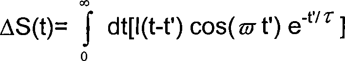
Mit
Bezug zu 16 wird nun ein alternativer phasenempfindlicher
Detektor beschrieben werden, der ohne ein Magnetfeld arbeitet. Mit
Bezug zu 16a werden regelmäßige Züge von ersten
und zweiten Steuerpulsen mit entgegengesetzten zirkularen Polarisationen
CP1a, CP1b etc.; CP2a, CP2b etc., dem optischen Schaltmedium derart
zugeführt, dass
der resultierende Spinzustand periodisch zwischen einem verhältnismäßig hohen
und niedrigen Niveau umgeschaltet wird, wie in 16b gezeigt ist. In 16c ist
ein Zug von Prüfpulsen
P1, P2, P3 bei drei verschiedenen Phasen Φ relativ zu der in 16b gezeigten Spinwellenform gezeigt. Relative Phasen
von Φ =
0, Φ =
n/2 und Φ =
n sind gezeigt. Die entsprechende Antwort vom Detektor, beispielsweise
dem Detektor 8 (aus 1) ist in 16d gezeigt. Man sieht, dass bei einer Phasendifferenz Φ = 0 die
Prüfpulse
einen positiven Nettospin erfassen werden, so dass der Detektor
eine positive Ausgabe liefern wird. Für Φ = n/2 wird die Detektorausgabe teilweise
positiv und teilweise negativ sein, was effektiv eine null-Ausgabe ergibt, wohingegen
für Φ = n ein negativer
Nettospin erfasst werden wird, was eine negative Ausgabe liefert.
Man sieht somit, dass die Detektorausgabe ein Spannungsniveau umfasst,
das zur phasenempfindlichen Detektion verwendet werden kann. Somit
kann die Detektorausgabe zum Ändern
der Phase der Prüfpulse
verwendet werden, um sie synchron zu den Steuerpulsen CP1, CP2 zu
halten.In reference to 16 Now, an alternative phase-sensitive detector will be described which operates without a magnetic field. In reference to 16a become regular trains of first and second control pulses with opposite circular polarizations CP1a, CP1b etc .; CP2a, CP2b, etc. are supplied to the optical switching medium such that the resulting spin state is periodically switched between a relatively high and low level, as in FIG 16b is shown. In 16c is a train of test pulses P1, P2, P3 at three different phases Φ relative to in 16b shown spin waveform shown. Relative phases of Φ = 0, Φ = n / 2 and Φ = n are shown. The corresponding response from the detector, such as the detector 8th (out 1 ) is in 16d shown. It can be seen that at a phase difference Φ = 0, the test pulses will detect a positive net spin so that the detector will provide a positive output. For Φ = n / 2, the detector output will be partially positive and partially negative, effectively giving zero output, whereas for Φ = n, a negative net spin will be detected, providing a negative output. It can thus be seen that the detector output comprises a voltage level that can be used for phase-sensitive detection. Thus, the detector output can be used to change the phase of the test pulses to keep them synchronous with the control pulses CP1, CP2.
16e zeigt einen Zug von Prüfpulsen mit einer Frequenz,
die von jener der Steuerpulse CP1, CP2 verschieden ist. Die entsprechende
Antwort ist in 16f gezeigt. Die durchschnittliche
Antwort ist null, wenn die Prüfpulse
keine Frequenzkomponente aufweisen, die ein Vielfaches der Frequenz
der Steuerpulse CP1, CP2 ist. Somit kann die Detektorausgabe verwendet
werden, um in die Frequenz der Steuerpulse einzurasten und dann
die Prüfpulse
in Phase mit den Steuerpulsen zu halten. 16e shows a train of test pulses having a frequency different from that of the control pulses CP1, CP2. The corresponding answer is in 16f shown. The average response is zero if the test pulses do not have a frequency component that is a multiple of the frequency of the control pulses CP1, CP2. Thus, the detector output can be used to lock into the frequency of the control pulses and then to keep the test pulses in phase with the control pulses.
Eine
weitere Verwendung dieser Erfindung ist als Zeit-Spannungs-Wandler. Wenn längere Prüfpulse verwendet
werden (einschließlich
im Grenzfall einem kontinuierlichen Wellenprüflaserstrahl), so wird die
integrierte Gesamtspindichte gemessen. Der ultraschnelle Anfangsstoß von biexcitonischen
Beiträgen
(siehe Heberle et al supra) für
beide Pulse löscht
sich aus. Der Nettospin ΔS,
der dann durch die Prüfstrahlung
gemessen wird ist dann gegeben durch wobei T = L/c die Zeit zwischen
zwei zu messenden Steuerpulsen ist, τ die Spinrelaxationszeit ist
(die wesentlich größer als
die zu messende Zeit sein muss, um innerhalb der linearen Approximation
zu bleiben), N die Zahl von Pulsen pro Sekunde ist und A die Kalibrationsspinamplitude
pro Puls ist. Dieses (elektronisch oder optisch) erfasste Prüfsignal
kann dann als Maß für die Zwischenpuls-Verzögerungszeit
verwendet werden.Another use of this invention is as a time-voltage converter. When longer test pulses are used (including, in the limit of a continuous wave test laser beam), the integrated total spin density is measured. The ultrafast initial burst of biecctic contributions (see Heberle et al supra) for both pulses quenches. The net spin ΔS, then through the Test radiation is measured is then given by where T = L / c is the time between two control pulses to be measured, τ is the spin relaxation time (which must be much greater than the time to be measured to stay within the linear approximation), N is the number of pulses per second, and A is the calibration spin amplitude per pulse. This (electronic or optical) detected test signal can then be used as a measure of the interpulse delay time.
Dieses
Prinzip kann verwendet werden, um Daten als Verzögerungszeiten zwischen zwei
Pulsen zu codieren. Mit Bezug zu 17 umfasst
ein schematisch gezeigter modengekoppelter Ringlaser 47 einen
optisch resonanten Ring 48 und einen elektro-optischen
Schalter und Polarisationswandler 49, der auf elektrische
Eingangsdaten anspricht, um aufeinanderfolgende rechts- und linkshändige zirkular polarisierte
Pulse CP1, CP2 zur Übertragung über einen
optischen Weg 50, beispielsweise eine optische Faser, zu
einem entfernten Detektor 51 zu erzeugen, der das optische
Schaltmedium 1 sowie einen Laser 52 enthält, welcher
einen kontinuierlichen (cw) Strahl von Prüfstrahlung 53 erzeugt.
Die Prüfstrahlung
wird auf ein Wollaston-Prisma 19 mit zugeordneten Detektoren 21a, 21b und
einem Verstärker 22 gerichtet, und
zwar in der mit Bezug zu 7 beschriebenen Weise. Die Datencodierung
ist in 18 gezeigt. Aufeinanderfolgende
numerische Werte werden in aufeinanderfolgenden Zeitrahmen Tf übertragen.
Jeder Zeitrahmen enthält
ein Paar der Pulse CP1, CP2 mit entgegengesetzter zirkularer Polarisation.
Die Verzögerung
zwischen den Pulsen gibt den numerischen Wert der Daten für den Zeitrahmen
an. Beim Detektor 47 wird für jeden Zeitrahmen Tf der Spinzustand des Schaltmediums 1 zunächst durch
den ersten Puls CP1 zu einem ersten Spinzustand geschaltet, und
danach durch den Puls CP2 zum zweiten Spinzustand geschaltet. Die
Verzögerung
zwischen den Pulsen ist eine Funktion des numerischen Werts der
Daten. die Polarisationsebene der Prüfstrahlung wird somit durch
die aufeinanderfolgenden Pulse CP1, CP2 zwischen zwei verschiedenen
Werten umgeschaltet, um elektrische Ausgangspulse auf der Leitung 23 zu
liefern, die eine Breite abhängig
vom Wert der für
jeden Zeitrahmen übertragenen
Daten haben. Das Übertragungsschema
hat den Vorteil, dass die übertragene
durchschnittliche optische Leistung verglichen mit herkömmlichen
Datenströmen konstant
ist, welche die Zahl von übertragenen
optischen Pulsen ändern.
Somit wird im Gegensatz zu herkömmlichen
Systemen jeder Heizeffekt beim optischen System auf einem niedrigen
Niveau gehalten und ist auf jeden Fall konstant, wodurch Nichtlinearitäten vermieden
werden, die als Folge einer Aufheizung durch die optischen Pulse
erzeugt werden können.
Um Daten über
lange optische Fasern zu übertragen
kann es ratsam sein, die Pulse für
jeden Zeitrahmen Tf in orthogonalen linearen
Polarisationen entlang einer die Polarisation beibehaltenden Faser zu übertragen,
und dann die Pulse am Faserende in zirkulare Polarisationen umzuwandeln.This principle can be used to encode data as delay times between two pulses. In reference to 17 comprises a schematically shown mode-locked ring laser 47 an optically resonant ring 48 and an electro-optical switch and polarization converter 49 responsive to electrical input data for sequential right and left handed circularly polarized pulses CP1, CP2 for transmission over an optical path 50 For example, an optical fiber, to a remote detector 51 to generate the optical switching medium 1 as well as a laser 52 containing a continuous (cw) beam of test radiation 53 generated. The test radiation is placed on a Wollaston prism 19 with associated detectors 21a . 21b and an amplifier 22 directed, in relation to 7 described way. The data encoding is in 18 shown. Successive numerical values are transmitted in successive time frames T f . Each time frame contains a pair of pulses CP1, CP2 of opposite circular polarization. The delay between pulses indicates the numerical value of the data for the time frame. At the detector 47 For each time frame T f, the spin state of the switching medium 1 first switched by the first pulse CP1 to a first spin state, and then switched by the pulse CP2 to the second spin state. The delay between pulses is a function of the numerical value of the data. the polarization plane of the test radiation is thus switched by the successive pulses CP1, CP2 between two different values, to electrical output pulses on the line 23 which have a width depending on the value of the data transmitted for each time frame. The transmission scheme has the advantage that the transmitted average optical power is constant compared to conventional data streams which change the number of transmitted optical pulses. Thus, unlike conventional systems, each heating effect in the optical system is kept at a low level and is in any case constant, thereby avoiding nonlinearities that can be generated as a result of heating by the optical pulses. In order to transmit data over long optical fibers, it may be advisable to transmit the pulses for each time frame T f in orthogonal linear polarizations along a polarization maintaining fiber, and then convert the pulses at the fiber end into circular polarizations.
Die
mit Bezug zu 1 beschriebene erfindungsgemäße Schaltvorrichtung
weist ein hervorragendes An-Aus-Kontrastverhältnis auf, da die Intensität von im
Aus-Zustand übertragenen
Licht nur durch das Polarisationsverhältnis des Polarisationsstrahlteilers 6 begrenzt
ist, welches 10–6 betragen kann.The related to 1 described switching device according to the invention has an excellent on-off contrast ratio, since the intensity of transmitted in the off-state light only by the polarization ratio of the polarization beam splitter 6 is limited, which may be 10 -6 .
Zahlreiche
Modifikationen und Variationen fallen in den Bereich der beanspruchten
Erfindung. Anstelle der Verwendung erster und zweiter Pulse mit entgegengesetzter
zirkularer Polarisation können beispielsweise
linear polarisierte orthogonale Steuerpulse verwendet werden, zusammen
mit einem Prüfpuls
mit 45° relativ
hierzu, um induzierte lineare Doppelbrechung zu detektieren, die
aus einer koherenten Überlagerung
der Spinzustände
resultiert. Als Referenz wird verwiesen auf "Transient Linear Birefringence in GaAs
Quantum Wells: Magnetic Field Dependence of Coherent Exciton Spin
Dynamics" R. E. Worsley
et al., Phys. Rev. Lett. 76, 3224 (1996).numerous
Modifications and variations are within the scope of the claimed claims
Invention. Instead of using first and second pulses with opposite
Circular polarization, for example
linearly polarized orthogonal control pulses are used together
with a test pulse
with 45 ° relative
in order to detect induced linear birefringence, the
from a coherent overlay
the spin states
results. For reference reference is made to "Transient Linear Birefringence in GaAs
Quantum Wells: Magnetic Field Dependence of Coherent Exciton Spin
Dynamics "R.E. Worsley
et al., Phys. Rev. Lett. 76, 3224 (1996).
Man
versteht somit aus dem Vorstehenden, dass erfindungsgemäße Schalter
in optischen Faserkommunikationssystemen mit geeignet ausgelegten InGaAsP-Vorrichtungen
im 1.3 μm-
und 1.5 μm-Wellenlängenband
eingesetzt werden können.
Der Schalter kann auch bei optischen Verbindungen zwischen Elektronikvorrichtungen
sowie in optischen Rechnern eingesetzt werden.you
thus understands from the above that switch according to the invention
in optical fiber communication systems with properly designed InGaAsP devices
in 1.3 μm
and 1.5 μm wavelength band
can be used.
The switch can also be used for optical connections between electronic devices
as well as in optical computers.