【0001】
【発明の属する技術分野】
本発明は、電子機器内に備えられたプリント配線板やケーブルから発生する、放射ノイズを抑制するシールドボックスに関するものである。
【0002】
【従来の技術】
近年、デジタル複写機や、デジタルプリンタ等の電子機器に搭載されるプリント配線板の駆動には高周波数の信号が使用され、プリント配線板自体やケーブル等から発生する不要な電磁波、所謂、放射ノイズが大きな問題となっている。そのため放射ノイズを防ぐために、プリント配線板やケーブルを金属筐体で覆い、シールドを形成する対策がとられている。これは、プリント配線板やケーブル上に流れる高周波電流から発生する電磁波を外部と遮蔽することを目的に行われ、シールドボックスを形成する導体上には、プリント配線板やケーブルの状態に応じた電流が流れる事になる。
【0003】
一般に、周波数が高くなると、導体上を流れる電流は、表皮効果によって、導体の表面のみを流れることになる。そのため、電子機器の動作に伴う様々な電気信号の送受信を行うプリント配線板やケーブルに対してシールドを施すと、シールドボックスを形成する導体の内側表面に電流が流れ、プリント配線板やケーブルから発生する電磁波を遮蔽する。
【0004】
しかしながら、シールドボックスで覆われたプリント配線板が単独で電子機器の機能を満たすことはほとんどなく、シールドボックスには、外部とのインターフェースとなるケーブルをシールドボックス内に引き込む開口部や、プリント配線板上のICなどから発生する熱を放熱するための開口部が必要となっている。シールドボックスに開口部が形成されることによって、高周波数の電流は、シールドボックスの外側の導体表面にも流れやすくなり、その結果、電磁波ノイズとして機器外に漏れ出てしまう。その上、シールドボックスに開口部が出来ると、開口部の大きさに応じて、共振現象が発生してしまうため、特定の周波数の放射ノイズが多量に漏れ出てしまう。
【0005】
例えば、図5に示すように直方体のシールドボックス1に、細長い四角形の開口部を設けた場合に、開口部がスロットアンテナとして作用し、特定の周波数が発生しやすくなる。開口部の長辺の長さxに対応して、(式1)に示す周波数fとその整数倍の周波数で、開口部に強い電界が発生しやすくなる。また、シールドボックス導体の開口部付近は、相互に打ち消しにくい電流分布となり、結果として、シールドボックスの遮蔽効果が作用せず、放射ノイズがでやすくなる。
【0006】
【外2】
【0007】
シールドボックスの開口部が原因となる放射ノイズを対策する従来の方法として、開口部の開口幅を短くする事が一般に知られている。これは、放射ノイズが問題として取り扱われる周波数(例えば30MHz〜1GHz)に対して、開口幅を短く設定することで、開口部がスロットアンテナとして作用する周波数を、より高周波数域に除外するものである。例えば、開口幅を15mm以下に設定する事により、スロットアンテナとして作用する周波数を1GHz以上にする事ができ、1GHz以下の放射ノイズの発生を抑制する事ができる。
【0008】
また、特開平8−32762に示すように、シールドボックスに設けられたCCDセンサーに画像光を走査露光するための開口から、CCDセンサーから放射されるノイズが漏れ出るのを防ぐため、シールドボックスの開口部の形状を筒状に変化させることで、共振現象を引き起こす周波数減衰させ、放射ノイズを抑制する手段が考えられている。
【0009】
【発明が解決しようとしている課題】
しかしながら、近年の電気信号の高速化に伴い、高調波成分も含めて電気信号の高周波化が進み、シールドボックスから漏れ出る電磁波の量も増加している。また、ICの高機能化に伴う回路規模の増大によって、プリント配線板自体の面積やケーブル配線数の増加を招いており、それを覆うシールドボックスの大きさも大きくなってきている。また、更にICの高速動作に伴う発熱量も増加しており、シールドボックスに作られる放熱用の開口部も大きくせざるを得ないのが現状である。
【0010】
前述した開口部からの放射ノイズだけでなく、空洞共振周波数によりシールドボックスから放射される放射ノイズの問題も顕在化している。空洞共振周波数は、シールドボックスの形状や材質特性などによって決まり、例えば、図6に示すような良導体で、各辺の長さがそれぞれX、Y、Zの直方体を形成している場合には、式(2)に示す周波数fboxで共振現象を引き起こすことになる。
【0011】
【外3】
この式で、m、n、pは伝播のモードを表している。fboxの最低周波数は、例えば(m,n,p)=(1,1,0)の時は式(3)で表され、その時の周波数でシールドの導体上には、定常的に打ち消されない電流分布が形成される。
【0012】
【外4】
【0013】
これは周波数fboxの整数倍の周波数でも同様に形成される。そのため、周波数fboxとその整数倍の周波数で放射ノイズが発生し、シールドボックスの遮蔽効果が作用しなくなる。
【0014】
空洞共振周波数によりシールドボックスから放射される放射ノイズは、シールドボックス全体から放射されるため、前記特開平8−32762に示された方法では、充分な対策はできない。逆に、空洞共振周波数はシールドボックスの形状により変化するため、ノイズの発生要因が複雑になり、解決が困難になってしまうという問題点もある。
【0015】
また、発生する放射ノイズの周波数は、設計された回路の配置や形状、配線方法、シールドボックスの形状等により決まり、通常、いくつかのピークとして現れる。従って、この放射ノイズのピークとなる周波数を効率的に減衰することが、電磁波ノイズ対策には重要であり望まれている。しかしながら前記特開平8−32762に示したような従来の方法は、所定範囲の周波数の放射ノイズを、所定の割合で減衰するものの、この特定のピークとなる周波数に対し、個別に対策をする事ができなかった。また、この最も対策しなければならない電磁波ノイズのピークとなる周波数は設計変更等があると大きく変化する。そのため、設計変更等に対応するためには、ローコストで簡単な構成での対策が望まれる。
【0016】
【課題を解決するための手段】
前記課題を解決するために本発明では、高周波デジタル信号を伝送するプリント配線板と、該プリント配線板を取り囲み、プリント配線板から放射される電磁波放射を減衰もしくは遮断する導電性シールドボックスにおいて、該プリント配線板から放射される特定の周波数の電磁波を吸収する、少なくとも1本の金属性のアンテナ部材を、該プリント配線板と導通していない状態で、シールドボックス内に配置した事により、シールドボックスから漏れ出る放射ノイズを抑制させている。
【0017】
また本発明では上記アンテナ部材を、減衰する周波数fに対して、
【外5】
(cは光速)の長さを持つ金属部材で構成する事により、シールドボックスの開口部から漏れ出る放射ノイズを抑制させている。
【0018】
また本発明では、前記減衰する周波数はシールドボックスの空洞共振周波数である事により、シールドボックスからの放射ノイズを抑制させている。
【0019】
また本発明では、前記アンテナ部材と、導電性のシールドボックスとは、特定のインピーダンスを有する素子で接続する事により、シールドボックスからの放射ノイズを抑制させている。
【0020】
また本発明では、前記インピーダンスを有する素子は、抵抗性を有することを特徴とする事により、シールドボックスからの放射ノイズを抑制させている。
【0021】
また本発明では、前記シールドボックスを備えた事を特徴とするシールドボックスを備えた電子機器を提供している。
【0022】
【発明の実施の形態】
次に、本発明の実施形態について説明する。
【0023】
本発明は、アンテナ部材が特定の周波数の電磁波を放射すると同時に、特定の周波数の電磁波を吸収する特性を利用し、シールドボックスから放射されるノイズを低減するものである。プリント配線板やケーブルなどを覆うシールドボックスの構成において、導体で形成されるシールドボックスの内部にプリント配線板やケーブルなどから発生する電磁波を、吸収するための金属製のアンテナ部材を形成し搭載する。
【0024】
まず、アンテナ部材を搭載することにより、シールドボックスから漏れ出る電磁波の総量を減らす原理について説明する。このアンテナ部材は、その長さを、式(4)に示す長さLに概略設定する事で、周波数fの電磁波を吸収する事が知られている。
【外6】
【0025】
従って、電子機器から発生する放射ノイズの周波数fに対応して、Lを設定する事で、プリント配線板などから発生する電磁波に対して、アンテナの相反性を利用して、搭載部材に電磁波を吸収する作用を持たせている。
【0026】
図6に示すシールドボックスの場合、問題となる周波数fopenは式(5)で示される。
【外7】
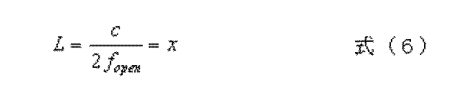
【0027】
このfopenに対してアンテナ部材の長さLは式(6)で示される。
【外8】
【0028】
また、開口幅が広く、アンテナ部材の長さLが長くなり、取り扱いに問題がある場合は、問題となる周波数fopenを、半波長に相当する周波数と、その倍数の周波数に設定することで、同等の効果が得られる。つまり吸収アンテナの長さを、x/2とする事により、シールドボックスから漏れ出る電磁波の量を緩和させ、機器外への放射ノイズを抑制させるものである。
【0029】
次に、シールドボックスの空洞共振周波数により問題となる周波数に関して説明する。図6に示すシールドボックスの場合、空洞共振周波数fboxは、式(7)に示す様に表せる。
【外9】
【0030】
このとき、fboxに対して、アンテナ部材の長さLは式(8)で示される。
【外10】
【0031】
シールドボックスの空洞共振周波数に対して、吸収アンテナがλ/2のアンテナとして作用するので、空洞共振周波数における放射ノイズのレベルを抑制することが出来る。
【0032】
次に、アンテナ部材がシールドボックス導体に、電気的導通がある接続を施す際には、アンテナ部材とシールドボックス導体との距離△∫を考慮する必要がある。これは、アンテナ部材とシールドボックスとをつなぐ導体部もアンテナ部材の一部として作用するためである。
【0033】
アンテナ部材の両端がシールドボックス導体に電気的導通がある接続を施す場合は、抑制する放射ノイズの周波数fに対して、式(9)に示す長さLに吸収アンテナの長さを設定する。この時はアンテナ部材の両側が接続することになるので、ほぼ1/2波長に対応する長さに設定する。
【外11】
【0034】
アンテナ部材の一端がシールドボックス導体に電気的導通がある接続を施す場合は、抑制する放射ノイズの周波数fに対して、式(10)に示す長さLに吸収アンテナの長さを設定する。この時はアンテナ部材の片側が接続することになるので、ほぼ1/4波長に対応する長さに設定する。
【外12】
【0035】
また、シールドボックス内に搭載されるプリント配線板上に、電気信号の動作に必要な配線導体とは別に、直流的に接続されていない配線導体を設ける事もできる。この場合には、プリント配線板等による配線導体の周囲の実効誘電率εと実効透磁率μを考慮する必要がある。
配線導体の長さLは放射ノイズの周波数fに対応して、式(11)に示す様に設定する。
【外13】
【0036】
以上の様にして、アンテナ部材を搭載することにより、シールドボックスから漏れ出る電磁波の総量を減らす事ができる。
【0037】
(第1の実施の形態)
図1は、本発明による第1の実施の形態を示すものであり、電子機器内のプリント配線板などに対して用いられるシールドボックスの部分を示したものである。図中1は概略直方体構造の導電性のシールドボックスである。直方体の各辺の長さは、X=300mm、Y=300mm、Z=300mmである。シールドボックス1内には、ネジ止め部2において固定されたプリント配線板3が収納されている。プリント配線板3は、画像処理や、レーザに関するICが実装されおり、基板上の配線には高周波電流が流れている。シールドボックス1には、長辺の長さx=100mm、短辺の長さy=5mmの開口部4が設けられている。プリント配線板3に接続するケーブル配線等は、開口部4を通って外部の基板や部品につなげられる。シールドボックス1の底面7には、アンテナ部材となる金属部材5が固定されている。金属部材5の材質は電気亜鉛メッキ鋼板である。
【0038】
図2は金属部材5のシールドボックス1の底面7への接続状態を示した図である。金属部材5は、不導体のネジ6でシールドボックス導体の底面7に不導体のスペーサー8を介して、接続固定されている。金属部材5の固定位置は、開口部4の近辺で、金属部材5の長さ方向と開口部の長辺とが平行になる様に設定されている。
【0039】
本実施形態では、この空洞共振周波数の放射ノイズを抑制する事を目的としている。このときシールドボックス1の空洞共振周波数は前述の式(6)より求められる。
【0040】
【外14】
【0041】
この周波数の放射ノイズを抑制するために、金属部材5の長さLは、式(7)より求められる。
【0042】
【外15】
金属部材5を使う事により、700MHzの周波数が大幅に減衰される。
【0043】
このように、前記に示された長さの金属部材5をシールドボックス1内に搭載することで、プリント配線板3上のデジタル信号動作によって流れる高周波成分の電流と、シールドボックス1との関係により発生し、高い放射ノイズレベルを引き起こす可能性がある、空洞共振周波数に概略相当する周波数と、その整数倍の周波数成分の電流が発生させる電磁波を吸収し、シールドボックスの外側に漏れ出る放射ノイズを抑制することができる。
【0044】
(第2の実施の形態)
図3は、本発明による第2の実施の形態を示すものであり、第1の実施の形態と同様のシールドボックス内に収納されるプリント配線板3の詳細部分を示したものである。プリント配線板3には、信号配線領域13が設けられておりIC10a、10bや外部との通信を行うコネクタ11などの電子部品、及びこれらの部品間に電気信号を伝送するための配線12があり実装されている。プリント配線板3上の信号配線領域13と電気的導通のない外側の部分には、長さLを持つ吸収アンテナ用配線14aを別途設けられている。プリント配線板3の実効誘電率は3、実効透磁率は1である。
【0045】
この時の吸収アンテナ用配線14aの長さLは、プリント配線板上におけるクロック信号などのデジタル信号によるノイズ周波数fに対して、式(10)より求める事ができる。空洞共振周波数のノイズfbox700MHzを抑制する場合の金属部材14aの長さL1は
【外16】
に設定する。
【0046】
以上のようにプリント配線板上に、アンテナ部材14aを配線することで、基板を配置後に別工程でアンテナ部材を組み立てる必要がなく、また基板成形時に同時にアンテナ部材14aを配線する事ができるため、製造タクトを短くする事ができ、製造コストおよび部品コストを安価にする事ができる。
【0047】
尚、本実施形態では、一本のアンテナ部材14aを用いたが、異なる周波数に対応するために、長さの異なる複数の吸収用配線を用いてもよい。また、配線の幅は、任意であってもよいし、配線周囲の誘電体や磁性体の特性は、プリント配線板3上の信号配線領域13と異なってもよい。
【0048】
(第3の実施の形態)
図4は、本発明による第3の実施の形態を示すものであり、第2の実施形態と同様のシールドボックス内に収納されるプリント配線板3の詳細部分を示したものであり、第2の実施形態と同じものは同じ符号を付してある。さらに、アンテナ部材14bの一端が、シールドボックスの導体と任意のインピーダンス特性を有した電気的接続が行えるように、ビスの接続穴15を設け、インピーダンス素子16が搭載されている。インピーダンス素子16を半田付けなどの方法で取付けられている。
【0049】
以上のような構成にする事で、アンテナ部材14bの長さを、プリント配線板上に十分な確保できない場合でも、インピーダンス素子でアンテナ部材14bの対応する長さを調整可能となり、所望の周波数に対応する事ができる。
【0050】
尚、本実施形態では、吸収用の配線14bの一端をインピーダンス素子でシールドボックス導体との接続を行ったが、両端や複数箇所に接続部を設けてもよい。また、複数のインピーダンス素子である一端を接続しても良い。
【0051】
【発明の効果】
以上説明したように、本発明によれば高周波デジタル信号を取り扱う電子機器において、シールドボックス内に金属性のアンテナ部材を備えるという簡単で安価な手段により、プリント配線板上のデジタル信号動作によって流れる高周波成分の電流により発生し、シールドボックス全体から空洞共振により放射される放射ノイズに対して、空洞共振周波数に概略相当する周波数と、その整数倍の周波数成分の電流が発生させる電磁波を吸収し、シールドボックスの外側に漏れ出る放射ノイズの量を抑制することができる。
【0052】
また、プリント配線板において、最も対策しなければならないノイズのピーク周波数を効率的に減衰する事である。また、安価で、製品設計上問題となるスペースを必要とせず、交換可能に取付ける事ができる。
【図面の簡単な説明】
【図1】第1の実施の形態を示す透過斜視図。
【図2】第1の実施の形態を説明する、シールドボックス内に配置する金属部材付近の拡大図。
【図3】第2の実施の形態を示す図。
【図4】第3の実施の形態を示す図。
【図5】従来の技術の示す図。
【図6】従来例の示す透過斜視図。
【符号の説明】
1 シールドボックス
2 ネジ止め部
3 プリント配線板
4 シールドボックス開口部
5 吸収用の金属性部材
6 不導体のネジ
7 シールドボックス導体の底面
8 不導体のスペーサー
10a、10b IC
11 コネクタ
12 配線
13 信号配線領域
14a、14b 吸収用の配線
15 接続穴
16 インピーダンス素子[0001]
TECHNICAL FIELD OF THE INVENTION
The present invention relates to a shield box for suppressing radiation noise generated from a printed wiring board or a cable provided in an electronic device.
[0002]
[Prior art]
In recent years, high-frequency signals have been used to drive printed wiring boards mounted on electronic devices such as digital copiers and digital printers, and unnecessary electromagnetic waves generated from the printed wiring boards themselves and cables, so-called radiated noise. Is a major problem. Therefore, in order to prevent radiation noise, measures have been taken to form a shield by covering the printed wiring board or cable with a metal housing. This is done to shield the electromagnetic waves generated from the high-frequency current flowing on the printed wiring board or cable from the outside.The conductors that form the shield box have a current corresponding to the state of the printed wiring board or cable. Will flow.
[0003]
In general, when the frequency increases, the current flowing on the conductor flows only on the surface of the conductor due to the skin effect. Therefore, if a printed circuit board or cable that transmits and receives various electrical signals in accordance with the operation of electronic equipment is shielded, a current flows on the inner surface of the conductor that forms the shield box and is generated from the printed circuit board and cable. To shield electromagnetic waves.
[0004]
However, the printed wiring board covered by the shield box rarely satisfies the functions of the electronic device alone, and the shield box has an opening for drawing a cable serving as an interface with the outside into the shield box, and a printed wiring board. An opening for dissipating heat generated from the upper IC or the like is required. By forming an opening in the shield box, a high-frequency current easily flows also on the conductor surface outside the shield box, and as a result, leaks out of the device as electromagnetic noise. In addition, if an opening is formed in the shield box, a resonance phenomenon occurs depending on the size of the opening, so that a large amount of radiation noise of a specific frequency leaks out.
[0005]
For example, when an elongated rectangular opening is provided in the rectangular parallelepiped shield box 1 as shown in FIG. 5, the opening acts as a slot antenna, and a specific frequency is easily generated. Corresponding to the length x of the long side of the opening, a strong electric field is easily generated in the opening at the frequency f shown in (Equation 1) and a frequency that is an integral multiple of the frequency f. Further, the current distribution near the opening of the shield box conductor is difficult to cancel each other out. As a result, the shielding effect of the shield box does not work, and radiation noise is likely to occur.
[0006]
[Outside 2]
As a conventional method for taking measures against radiation noise caused by the opening of the shield box, it is generally known to reduce the opening width of the opening. This is to set the aperture width shorter than the frequency (for example, 30 MHz to 1 GHz) where radiation noise is treated as a problem, thereby excluding the frequency at which the aperture acts as a slot antenna into a higher frequency range. is there. For example, by setting the opening width to 15 mm or less, the frequency acting as a slot antenna can be 1 GHz or more, and the generation of radiation noise of 1 GHz or less can be suppressed.
[0008]
Further, as disclosed in JP-A-8-32762, in order to prevent noise radiated from the CCD sensor from leaking from an opening for scanning and exposing image light to a CCD sensor provided in the shield box, a shield box is provided. Means of changing the shape of the opening into a cylindrical shape to attenuate the frequency that causes a resonance phenomenon and suppress radiation noise have been considered.
[0009]
[Problems to be solved by the invention]
However, with the recent increase in the speed of electric signals, the frequency of electric signals including harmonic components has been increased, and the amount of electromagnetic waves leaking from the shield box has also increased. In addition, an increase in the circuit scale accompanying the sophistication of the IC has caused an increase in the area of the printed wiring board itself and the number of cable wirings, and the size of a shield box for covering the same has also been increasing. Further, the amount of heat generated by the high-speed operation of the IC is also increasing, and at present, the heat radiation opening formed in the shield box has to be enlarged.
[0010]
In addition to the radiation noise from the opening described above, the problem of radiation noise radiated from the shield box due to the cavity resonance frequency has also become apparent. The cavity resonance frequency is determined by the shape and material characteristics of the shield box. For example, in the case of a good conductor as shown in FIG. 6, when the length of each side is X, Y and Z, respectively, A resonance phenomenon is caused at the frequency f box shown in Expression (2).
[0011]
[Outside 3]
In this equation, m, n, and p represent modes of propagation. The lowest frequency of the f box is expressed, for example, by (3) when (m, n, p) = (1, 1, 0), and is constantly canceled on the shield conductor at the frequency at that time. No current distribution is formed.
[0012]
[Outside 4]
[0013]
This is similarly formed at a frequency that is an integral multiple of the frequency f box . Therefore, radiation noise occurs at the frequency f box and a frequency that is an integral multiple of the frequency f box, and the shielding effect of the shielding box does not work.
[0014]
Since the radiation noise radiated from the shield box due to the cavity resonance frequency is radiated from the entire shield box, a sufficient measure cannot be taken by the method disclosed in the above-mentioned Japanese Patent Application Laid-Open No. 8-32762. Conversely, since the cavity resonance frequency changes depending on the shape of the shield box, there is a problem that the factor of noise generation becomes complicated and the solution becomes difficult.
[0015]
The frequency of the generated radiation noise is determined by the layout and shape of the designed circuit, the wiring method, the shape of the shield box, and the like, and usually appears as several peaks. Therefore, it is important and desired to effectively attenuate the peak frequency of the radiation noise in order to prevent electromagnetic noise. However, in the conventional method as disclosed in Japanese Patent Application Laid-Open No. 8-32762, radiation noise in a predetermined range of frequencies is attenuated at a predetermined ratio, but individual measures are taken against the specific peak frequency. Could not. Further, the frequency at which the peak of the electromagnetic wave noise, which must be dealt with most, greatly changes when there is a design change or the like. Therefore, in order to cope with a design change or the like, a measure with a low-cost and simple configuration is desired.
[0016]
[Means for Solving the Problems]
In order to solve the above problems, in the present invention, a printed wiring board for transmitting a high-frequency digital signal, and a conductive shield box surrounding the printed wiring board and attenuating or blocking electromagnetic wave radiation radiated from the printed wiring board, By arranging at least one metallic antenna member that absorbs electromagnetic waves of a specific frequency radiated from the printed wiring board in a shield box in a state where it is not electrically connected to the printed wiring board, The radiated noise leaking out from is suppressed.
[0017]
Further, in the present invention, the antenna member is moved with respect to a frequency f to be attenuated.
[Outside 5]
The radiation noise leaking from the opening of the shield box is suppressed by using a metal member having a length (c is the speed of light).
[0018]
Further, in the present invention, since the attenuating frequency is the cavity resonance frequency of the shield box, the radiation noise from the shield box is suppressed.
[0019]
Further, in the present invention, the antenna member and the conductive shield box are connected by an element having a specific impedance, thereby suppressing radiation noise from the shield box.
[0020]
Further, in the present invention, the element having the impedance has resistance, thereby suppressing radiation noise from the shield box.
[0021]
Further, the present invention provides an electronic device provided with a shield box, wherein the electronic device is provided with the shield box.
[0022]
BEST MODE FOR CARRYING OUT THE INVENTION
Next, an embodiment of the present invention will be described.
[0023]
The present invention reduces the noise radiated from a shield box by utilizing the characteristic that an antenna member radiates an electromagnetic wave of a specific frequency and simultaneously absorbs an electromagnetic wave of a specific frequency. In a shield box configuration that covers printed wiring boards and cables, a metal antenna member for absorbing electromagnetic waves generated from printed wiring boards and cables is formed and mounted inside a shield box made of conductors. .
[0024]
First, the principle of reducing the total amount of electromagnetic waves leaking from the shield box by mounting an antenna member will be described. It is known that this antenna member absorbs an electromagnetic wave of frequency f by roughly setting its length to the length L shown in Expression (4).
[Outside 6]
[0025]
Therefore, by setting L according to the frequency f of the radiated noise generated from the electronic device, the electromagnetic wave generated from the printed wiring board or the like is used to apply the electromagnetic wave to the mounting member by utilizing the reciprocity of the antenna. Has the effect of absorbing.
[0026]
In the case of the shield box shown in FIG. 6, the problematic frequency f open is expressed by equation (5).
[Outside 7]
[0027]
The length L of the antenna member with respect to this f open is represented by Expression (6).
[Outside 8]
[0028]
When the aperture width is wide and the length L of the antenna member is long and there is a problem in handling, the problematic frequency f open is set to a frequency corresponding to a half wavelength and a frequency that is a multiple of the half wavelength. The same effect can be obtained. In other words, by setting the length of the absorbing antenna to x / 2, the amount of electromagnetic waves leaking from the shield box is reduced, and radiation noise to the outside of the device is suppressed.
[0029]
Next, a description will be given of a frequency that becomes a problem due to the cavity resonance frequency of the shield box. In the case of the shield box shown in FIG. 6, the cavity resonance frequency f box can be expressed as shown in Expression (7).
[Outside 9]
[0030]
At this time, the length L of the antenna member with respect to f box is represented by Expression (8).
[Outside 10]
[0031]
Since the absorption antenna functions as an antenna of λ / 2 with respect to the cavity resonance frequency of the shield box, the level of radiation noise at the cavity resonance frequency can be suppressed.
[0032]
Next, when the antenna member connects the shield box conductor with electrical conduction, it is necessary to consider the distance と between the antenna member and the shield box conductor. This is because the conductor connecting the antenna member and the shield box also acts as a part of the antenna member.
[0033]
When both ends of the antenna member are connected to the shield box conductor with electrical conduction, the length of the absorbing antenna is set to the length L shown in Expression (9) with respect to the frequency f of the radiation noise to be suppressed. At this time, since both sides of the antenna member are connected, the length is set to substantially correspond to a half wavelength.
[Outside 11]
[0034]
When one end of the antenna member is connected to the shield box conductor so as to be electrically conductive, the length of the absorbing antenna is set to the length L shown in Expression (10) with respect to the frequency f of the radiated noise to be suppressed. At this time, since one side of the antenna member is connected, the length is set to approximately one quarter wavelength.
[Outside 12]
[0035]
In addition, on a printed wiring board mounted in the shield box, a wiring conductor that is not DC-connected can be provided separately from a wiring conductor required for operation of an electric signal. In this case, it is necessary to consider the effective permittivity ε and the effective magnetic permeability μ around the wiring conductor formed by a printed wiring board or the like.
The length L of the wiring conductor is set as shown in Expression (11), corresponding to the frequency f of the radiation noise.
[Outside 13]
[0036]
As described above, by mounting the antenna member, the total amount of electromagnetic waves leaking from the shield box can be reduced.
[0037]
(First Embodiment)
FIG. 1 shows a first embodiment of the present invention, and shows a portion of a shield box used for a printed wiring board or the like in an electronic device. In the figure, reference numeral 1 denotes a conductive shield box having a substantially rectangular parallelepiped structure. The length of each side of the rectangular parallelepiped is X = 300 mm, Y = 300 mm, and Z = 300 mm. In the shield box 1, a printed wiring board 3 fixed at the screwing portion 2 is housed. The printed wiring board 3 has an IC for image processing and laser mounted thereon, and a high-frequency current flows through the wiring on the substrate. The shield box 1 is provided with an opening 4 having a long side length x = 100 mm and a short side length y = 5 mm. Cable wiring or the like connected to the printed wiring board 3 is connected to an external board or component through the opening 4. A metal member 5 serving as an antenna member is fixed to a bottom surface 7 of the shield box 1. The material of the metal member 5 is an electrogalvanized steel plate.
[0038]
FIG. 2 is a diagram showing a connection state of the metal member 5 to the bottom surface 7 of the shield box 1. The metal member 5 is connected and fixed to the bottom surface 7 of the shield box conductor via a nonconductive spacer 8 with a nonconductive screw 6. The fixing position of the metal member 5 is set near the opening 4 such that the length direction of the metal member 5 and the long side of the opening are parallel.
[0039]
The purpose of the present embodiment is to suppress the radiation noise at the cavity resonance frequency. At this time, the cavity resonance frequency of the shield box 1 can be obtained from the above equation (6).
[0040]
[Outside 14]
[0041]
In order to suppress the radiation noise of this frequency, the length L of the metal member 5 is obtained from Expression (7).
[0042]
[Outside 15]
By using the metal member 5, the frequency of 700 MHz is greatly attenuated.
[0043]
In this manner, by mounting the metal member 5 having the length shown above in the shield box 1, the relationship between the current of the high-frequency component flowing by the digital signal operation on the printed wiring board 3 and the shield box 1 is increased. Generates and may cause a high radiation noise level. It absorbs electromagnetic waves generated by currents of frequency components roughly equivalent to the cavity resonance frequency and frequency components that are integral multiples of the resonance frequency, and emits radiation noise that leaks out of the shield box. Can be suppressed.
[0044]
(Second embodiment)
FIG. 3 shows a second embodiment according to the present invention, and shows a detailed portion of a printed wiring board 3 housed in a shield box similar to the first embodiment. The printed wiring board 3 is provided with a signal wiring area 13 and includes electronic components such as ICs 10a and 10b and a connector 11 for communicating with the outside, and wiring 12 for transmitting an electric signal between these components. Has been implemented. Absorbing antenna wiring 14a having a length L is separately provided on an outer portion of the printed wiring board 3 which is not electrically connected to the signal wiring area 13. The effective permittivity of the printed wiring board 3 is 3, and the effective magnetic permeability is 1.
[0045]
The length L of the wiring 14a for the absorbing antenna at this time can be obtained from the equation (10) with respect to the noise frequency f due to a digital signal such as a clock signal on the printed wiring board. The length L1 of the metal member 14a when suppressing the resonance fbox 700MHz of the cavity resonance frequency is as follows.
Set to.
[0046]
By arranging the antenna member 14a on the printed wiring board as described above, there is no need to assemble the antenna member in a separate process after the substrate is placed, and the antenna member 14a can be wired at the same time when the substrate is formed. Manufacturing tact can be shortened, and manufacturing cost and parts cost can be reduced.
[0047]
In the present embodiment, one antenna member 14a is used, but a plurality of absorption wires having different lengths may be used to correspond to different frequencies. Further, the width of the wiring may be arbitrary, and the characteristics of the dielectric and magnetic materials around the wiring may be different from those of the signal wiring region 13 on the printed wiring board 3.
[0048]
(Third embodiment)
FIG. 4 shows a third embodiment according to the present invention, and shows a detailed portion of a printed wiring board 3 housed in a shield box similar to the second embodiment. The same reference numerals are given to the same components as those of the embodiment. Further, a screw connection hole 15 is provided and an impedance element 16 is mounted so that one end of the antenna member 14b can be electrically connected to the conductor of the shield box with an arbitrary impedance characteristic. The impedance element 16 is attached by a method such as soldering.
[0049]
With the above configuration, even when the length of the antenna member 14b cannot be sufficiently secured on the printed wiring board, the corresponding length of the antenna member 14b can be adjusted by the impedance element, and the desired frequency can be obtained. Can respond.
[0050]
In the present embodiment, one end of the absorption wiring 14b is connected to the shield box conductor by an impedance element, but connection portions may be provided at both ends and at a plurality of locations. Further, one end which is a plurality of impedance elements may be connected.
[0051]
【The invention's effect】
As described above, according to the present invention, in an electronic device that handles a high-frequency digital signal, a high-frequency current flowing by a digital signal operation on a printed wiring board is provided by a simple and inexpensive means of providing a metal antenna member in a shield box. For the radiated noise generated by the current of the component and radiated from the whole shield box by the cavity resonance, the electromagnetic wave generated by the current of the frequency component approximately equivalent to the cavity resonance frequency and an integral multiple of the frequency is absorbed and shielded. The amount of radiation noise leaking out of the box can be suppressed.
[0052]
Another object of the present invention is to efficiently attenuate the peak frequency of noise, which must be taken the most in a printed wiring board. In addition, it can be mounted inexpensively and replaceably without requiring a space which is a problem in product design.
[Brief description of the drawings]
FIG. 1 is a transparent perspective view showing a first embodiment.
FIG. 2 is an enlarged view of the vicinity of a metal member arranged in a shield box, for explaining the first embodiment.
FIG. 3 is a diagram showing a second embodiment.
FIG. 4 is a diagram showing a third embodiment.
FIG. 5 is a diagram showing a conventional technique.
FIG. 6 is a transparent perspective view showing a conventional example.
[Explanation of symbols]
DESCRIPTION OF SYMBOLS 1 Shield box 2 Screw part 3 Printed wiring board 4 Shield box opening 5 Absorbing metallic member 6 Non-conductive screw 7 Bottom of shield box conductor 8 Non-conductive spacer 10a, 10b IC
DESCRIPTION OF SYMBOLS 11 Connector 12 Wiring 13 Signal wiring area 14a, 14b Wiring for absorption 15 Connection hole 16 Impedance element