Background
With the increasing data processing speed of modern Digital systems, the importance of high-performance Analog-to-Digital converters (ADCs) is increasing. High-speed high-precision ADC is usually realized by adopting a switched capacitor circuit and a step-by-step conversion structure, such as pipeline, SAR, Subridge SAR and the like, and in order to optimize noise and power consumption, an input sampling holding amplifier at the front end is cancelled, so that a signal directly enters a first-step conversion circuit. Fig. 1 is a schematic block diagram of a conventional Switched Capacitor Analog-to-Digital Converter system, in which a second Analog-to-Digital Converter and a Switched Capacitor Digital-to-Analog Converter SC DAC (Switched Capacitor Digital-Analog Converter) form a first-step conversion circuit, i.e., a front-end circuit. Fig. 2 is a schematic diagram of a specific circuit implementation of the front-end circuit formed by the second analog-to-digital converter and the switched capacitor DAC in fig. 1. Input signal VinThe two parts are used for sampling simultaneously, one part is a sampling capacitor C in the rough division ADCc1~CcmOne path is a sampling capacitor C in the SC DAC1~Cm. After sampling, the circuit enters the conversion stage of a second analog-to-digital converter, C in the second analog-to-digital converterc1~CcmBottom plate switching to reference voltage Vr1~VrmThe comparator is triggered to obtain an output result Q1~Qm. As shown in FIG. 2, when the circuit enters the D/A conversion state, the result Q is outputted1~QmSeparately controlling SC DAC capacitors C1~CmBottom plate connects VrefpOr VrefnThe SC DAC converts the result Q according to the second analog-to-digital converter in the previous step1~QmObtaining an analog residual difference signal VEAnd takes it as the input value of the first analog-to-digital converter.
It is apparent, however, that, in the absence of a front-end sample-and-hold amplifier,after an input signal directly enters a first-step conversion circuit, a traditional switched capacitor analog-to-digital converter front-end circuit has two sampling paths, and in order to ensure that the values of the two acquired input signals are the same, two time constants are required to be completely the same and the sampling time is not deviated. However, in practical circuit implementation, due to the influence of factors such as design, process, layout, and the like, complete matching between two paths is impossible, and input signal values obtained by tracking and sampling the two paths have a deviation, namely, an aperture error, which affects the conversion accuracy of the analog-to-digital converter and even causes a conversion error after exceeding a certain amount. Also, the aperture error is related to the input signal frequency, and the higher the frequency signal frequency, the larger the error, so it actually limits the input signal bandwidth of the ADC. In addition, the input capacitance is also an important index of the ADC, and is a load presented to the ADC driver by the ADC, representing the difficulty of driving the ADC driver, and the larger the input capacitance, the harder it is to be driven, and the harder it is to achieve broadband performance. As shown in FIG. 2, the input capacitance of the conventional front-end circuit can be represented as
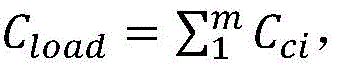
I.e. the second analog-to-digital converter and the sampling network of the SC DAC both constitute a load for the input signal.
Disclosure of Invention
The object of the present invention is to solve at least to some extent one of the above mentioned technical problems.
Therefore, a first objective of the present invention is to provide an input sampling and converting circuit, which employs capacitance multiplexing, combines two sampling paths of a conventional switched capacitor analog-to-digital converter front-end circuit into one sampling path, and has the advantages of reducing aperture error, reducing input signal load, and optimizing chip area.
To achieve the above object, an embodiment of a first aspect of the present invention provides an input sampling and converting circuit, including: m sampling capacitors (C)C1~CCm) M comparators, m being a positive integer, wherein: the m sampling capacitors (C)C1~CCm) Respectively pass through the firstClock phase ck1 connected to input voltage VinThe bottom plates of the m sampling capacitors are respectively connected with a reference voltage V through a second clock phase ck2r1~VrmThe top plates of the m sampling capacitors are respectively connected with the input ends of the m comparators, and the output ends of the m comparators output conversion results Q1~Qm(ii) a The conversion result Q1~QmThe bottom plate of the corresponding capacitor is controlled to be connected with V through the third clock phase ck3refpOr VrefnThe top plates of the corresponding capacitors are connected in parallel through the third clock phase ck3 to obtain VE(ii) a The V isEAs an input to the first analog-to-digital converter.
According to the input sampling and conversion circuit of the embodiment of the invention, m sampling capacitors (C) are usedC1~CCm) Respectively connected with an input voltage VinOutputs the conversion result Q1~Qm(ii) a Conversion result Q1~QmBottom plate connection V for respectively controlling corresponding capacitorsrefpOr VrefnAll the top plates of the corresponding capacitors are connected in parallel to obtain VE;VEAs an input to the first analog-to-digital converter. Capacitance (C)C1~CCm) Multiplexing to the second analog-to-digital converter and the SC DAC has the advantages of reducing aperture error, reducing input signal load, and optimizing chip area.
In one embodiment of the invention, the first clock phase ck1 is in a high input signal sampling state, the second clock phase ck2 is in a high second analog-to-digital converter conversion state, and the third clock phase ck3 is in a high D/A conversion state and a fine A/D conversion state.
In one embodiment of the invention, the difference between the inputs of the second adc comparator is the input voltage VinAnd a threshold voltage VcmThe difference of (a).
In one embodiment of the present invention, the output terminals of the m comparators output the conversion result Q1~Qm。
In one embodiment of the present invention, the second clock phase ck2 rises when the first clock phase ck1 falls, and the third clock phase ck3 rises when the second clock phase ck2 falls.
In one embodiment of the present invention, when the first clock phase ck1 is high, the circuit enters a sampling state, and the input capacitance of the circuit is
M is the number of capacitors in the circuit, and the bottom plate of the capacitor is connected with an input voltage V
in。
In an embodiment of the present invention, when the second clock phase ck2 is at a high level, the circuit enters a second analog-to-digital converter conversion state, and the bottom plates of the capacitors of the circuit are respectively connected to the corresponding reference levels to obtain a conversion result Q1~Qm。
In one embodiment of the present invention, when the third clock phase ck3 is high, the circuit enters a D/a conversion state, and the conversion result Q is1~QmBottom plate connection V for respectively controlling corresponding capacitorsrefpOr VrefnAll the top plates of the corresponding capacitors are connected in parallel to obtain VE
Additional aspects and advantages of the invention will be set forth in part in the description which follows and, in part, will be obvious from the description, or may be learned by practice of the invention.
Detailed Description
Reference will now be made in detail to embodiments of the present invention, examples of which are illustrated in the accompanying drawings, wherein like or similar reference numerals refer to the same or similar elements or elements having the same or similar function throughout. The embodiments described below with reference to the drawings are illustrative and intended to be illustrative of the invention and are not to be construed as limiting the invention.
An input sampling and conversion circuit according to an embodiment of the present invention is described below with reference to the drawings.
Fig. 3 is a diagram of an input sampling and conversion front-end circuit according to an embodiment of the present invention.
Fig. 4 is a control timing diagram of an input sampling and conversion front-end circuit according to an embodiment of the present invention.
As shown in fig. 3, the input sampling and conversion front-end circuit diagram may include: m sampling capacitors (C)C1~CCm) M comparators, m being a positive integer.
Wherein, m sampling capacitors CC1~CCmRespectively connected to an input voltage V through switches controlled by a first clock phase ck1inM sampling capacitors (C)C1~CCm) Are respectively connected with a reference voltage V through switches controlled by a second clock phase ck2r1~VrmThe top plates of the m sampling capacitors are respectively connected with the input ends of the m comparators, and the output ends of the comparators output conversion results Q1~Qm。
Conversion result Q1~QmThe corresponding capacitances (C) are controlled by the third clock phase ck3 respectivelyC1~CCm) Bottom plate of (2) is connected with VrefpOr VrefnThe top plate of the corresponding capacitor is connected in parallel through a switch controlled by a third clock phase ck3 to obtain VE。
VEAs an input to the first analog-to-digital converter. Wherein the first analog-to-digital converter can be a high-precision analog-to-digital converter.
It should be noted that m is determined by the accuracy of the second adc, for example, the second adc is N bits, and m is 2N-1, in particular, the second moldThe number of the digital converters is 2 bits, the number of the sampling capacitors is 3, and the number of the comparators is 3. The accuracy of the second analogue to digital converter can be set as desired. Wherein the second analog-to-digital converter may be a relatively low accuracy analog-to-digital converter.
Specifically, according to the control timing chart of fig. 4, the analog-to-digital converter is divided into 4 operating states: the input signal sample state with clock ck1 high, the second analog to digital converter transition state with clock ck2 high, the D/A transition state with clock ck3 high and the subsequent fine A/D transition state.
In the sample state, clock ck1 is high and capacitor C is set
c1~C
cmThe bottom plate is connected with an input signal, the top plate is connected with a common-mode voltage, and the input capacitance is
When the ck1 is low, the sampling is finished, the circuit enters a second analog-to-digital converter conversion state, the clock ck2 is high, and the sampling capacitor Cc1~CcmThe bottom plates are respectively connected with corresponding reference levels Vr1~VrmThe second A/D converter starts to work to obtain m conversion results Q of the high-order section at one time1~Qm。
When the second adc comparison is complete, the circuit goes to the D/a conversion state, clock ck3 is high, capacitor C is shown in fig. 3c1~CcmThe bottom plates are respectively in the conversion result Q1~QmUnder the control of (V)refpOr VrefnCapacitor Cc1~CcmThe top plates are all connected in parallel to obtain a simulated residual error signal VEAnd the comparison is carried out on the next lower section by taking the lower section as the input of the first analog-to-digital converter.
The input sampling and conversion front-end circuit multiplexes the second analog-to-digital converter capacitor and the traditional SC DAC capacitor, so that an independent second analog-to-digital converter sampling network in the traditional design is degenerated into the SC DAC, and the aperture error effect and the input signal load are effectively reduced.
It can be understood that, in the input sampling and converting circuit according to the embodiment of the present invention, the sampling capacitor of the second analog-to-digital converter is degenerated with the SC DAC capacitor, and the signal sampled by the capacitor network of the second analog-to-digital converter is used for both a/D conversion and D/a conversion, so that the problem of aperture error between the sampling capacitor of the second analog-to-digital converter and the SC DAC capacitor can be avoided.
It should be noted that, in the embodiment of the present invention, the first clock phase ck1 is in the high input signal sampling state, the second clock phase ck2 is in the high second analog-to-digital converter conversion state, the third clock phase ck3 is in the high D/a conversion state and the fine a/D conversion state, a specific description of each clock phase is shown in fig. 4, and the analog-to-digital converter is divided into 4 operating states.
According to the input sampling and conversion circuit of the embodiment of the invention, m sampling capacitors (C) are usedC1~CCm) Respectively connected with an input voltage VinOutputs the conversion result Q1~Qm(ii) a Conversion result Q1~QmRespectively controlling the capacitance (C)C1~CCm) Bottom plate of (2) is connected with VrefpOr VrefnAll the top plates of the capacitors are connected in parallel to obtain VE;VEAs an input to the first analog-to-digital converter. The method has the advantages of reducing aperture errors, reducing input signal load and optimizing chip area.
In the description of the present invention, it is to be understood that the terms "first", "second" and the like are used for descriptive purposes only and are not to be construed as indicating or implying relative importance or implying any number of technical features indicated. Thus, a feature defined as "first" or "second" may explicitly or implicitly include at least one such feature.
In the description herein, references to the description of the term "one embodiment," "some embodiments," "an example," "a specific example," or "some examples," etc., mean that a particular feature, structure, material, or characteristic described in connection with the embodiment or example is included in at least one embodiment or example of the invention. In this specification, the schematic representations of the terms used above are not necessarily intended to refer to the same embodiment or example. Furthermore, the particular features, structures, materials, or characteristics described may be combined in any suitable manner in any one or more embodiments or examples. Furthermore, various embodiments or examples and features of different embodiments or examples described in this specification can be combined and combined by one skilled in the art without contradiction.
Although embodiments of the present invention have been shown and described above, it is understood that the above embodiments are exemplary and should not be construed as limiting the present invention, and that variations, modifications, substitutions and alterations can be made to the above embodiments by those of ordinary skill in the art within the scope of the present invention.